


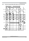
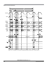
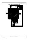

Appendix C Recommended PCB Layout
MC9S12XDP512 Data Sheet, Rev. 2.11
Freescale Semiconductor 969
Appendix C
Recommended PCB Layout
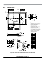
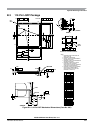
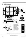
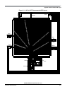
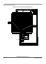
The PCB must be carefully laid out to ensure proper operation of the voltage regulator as well as of the
MCU itself. The following rules must be observed:
• Every supply pair must be decoupled by a ceramic capacitor connected as near as possible to the
corresponding pins (C1–C6).
• Central point of the ground star should be the V
SSR
pin.
• Use low ohmic low inductance connections between V
SS1
, V
SS2
, and V
SSR
.
•V
SSPLL
must be directly connected to V
SSR
.
• Keep traces of V
SSPLL
, EXTAL, and XTAL as short as possible and occupied board area for C7,
C8, and Q1 as small as possible.
• Do not place other signals or supplies underneath area occupied by C7, C8, and Q1 and the
connection area to the MCU.
• Central power input should be fed in at the V
DDA
/V
SSA
pins.