


Chapter 17 Voltage Regulator (S12VREG3V3V5)
MC9S12XDP512 Data Sheet, Rev. 2.11
736 Freescale Semiconductor
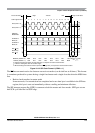
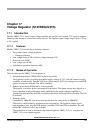
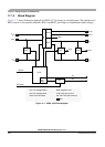
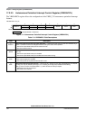
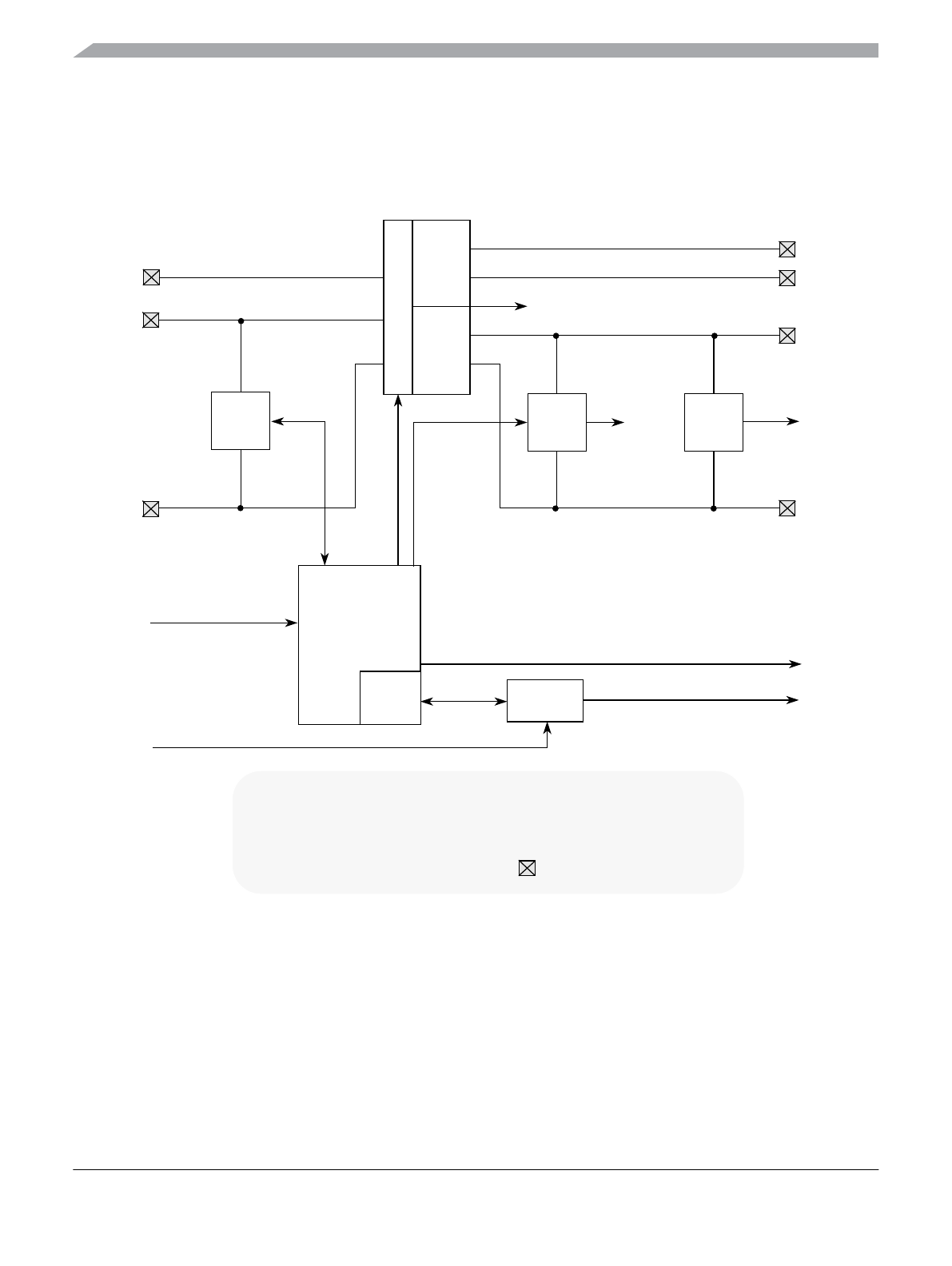
17.1.3 Block Diagram
Figure 17-1 shows the function principle of VREG_3V3 by means of a block diagram. The regulator core
REG consists of two parallel subblocks, REG1 and REG2, providing two independent output voltages.
Figure 17-1. VREG_3V3 Block Diagram
LVR
LVD
POR
V
DDR
V
DD
LVI
POR
LVR
CTRL
V
SS
V
DDPLL
V
SSPLL
V
REGEN
REG
REG2
REG1
PIN
V
DDA
V
SSA
REG: Regulator Core
CTRL: Regulator Control
LVD: Low-Voltage Detect
LVR: Low-Voltage Reset
POR: Power-On Reset
API
API
API: Auto. Periodical Interrupt
VBG
API
Rate
Select
Bus Clock