


Chapter 20 Debug (S12XDBGV2)
MC9S12XDP512 Data Sheet, Rev. 2.11
Freescale Semiconductor 823
20.4.5.3.1 Information Byte Organization
The format of the control information byte for both CPU and XGATE modules is dependent upon the
active trace mode and tracing source as described below. In normal mode or loop1 mode, tracing of
XGATE activity XINF is used to store control information. In normal mode or loop1 mode, tracing of CPU
activity CINF is used to store control information. In detail mode, CXINF contains the control information.
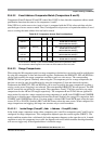
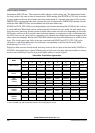
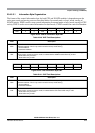
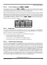
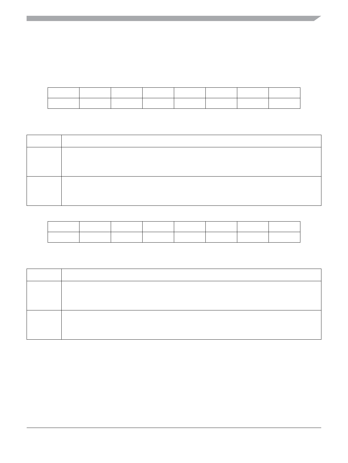
Bit 7 Bit 6 Bit 5 Bit 4 Bit 3 Bit 2 Bit 1 Bit 0
XSD00XDV0000
Figure 20-24. XGATE Information Byte XINF
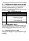
Table 20-40. XINF Field Descriptions
Field Description
7
XSD
Source Destination Indicator — This bit indicates if the corresponding stored address is a source or
destination address. This is only used in normal and loop1 mode tracing.
0 Source Address
1 Destination Address
4
XDV
Data Invalid Indicator — This bit indicates if the trace buffer entry is invalid. It is only used when tracing from
both sources in normal and loop1 mode, to indicate that the XGATE trace buffer entry is valid.
0 Trace buffer entry is invalid
1 Trace buffer entry is valid
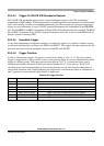
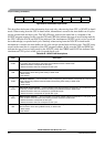
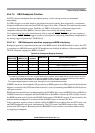
Bit 7 Bit 6 Bit 5 Bit 4 Bit 3 Bit 2 Bit 1 Bit 0
CSD00CDV0000
Figure 20-25. CPU Information Byte CINF
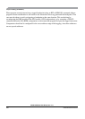
Table 20-41. CINF Field Descriptions
Field Description
7
CSD
Source Destination Indicator — This bit indicates if the corresponding stored address is a source or
destination address. This is only used in normal and loop1 mode tracing.
0 Source Address
1 Destination Address
4
CDV
Data Invalid Indicator — This bit indicates if the trace buffer entry is invalid. It is only used when tracing from
both sources in normal and loop1 mode, to indicate that the CPU trace buffer entry is valid.
0 Trace buffer entry is invalid
1 Trace buffer entry is valid