


Chapter 19 Background Debug Module (S12XBDMV2)
MC9S12XDP512 Data Sheet, Rev. 2.11
Freescale Semiconductor 769
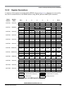
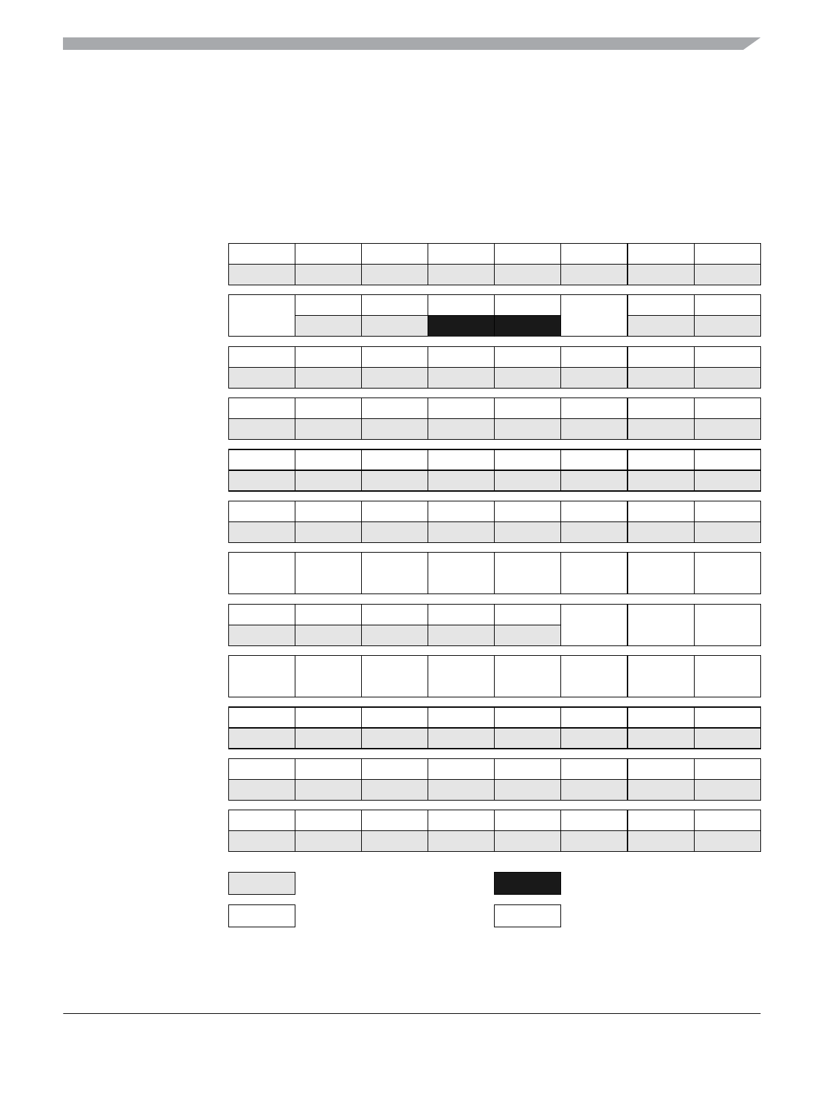
19.3.2 Register Descriptions
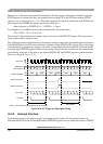
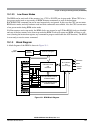
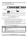
A summary of the registers associated with the BDM is shown in Figure 19-2. Registers are accessed by
host-driven communications to the BDM hardware using READ_BD and WRITE_BD commands.
Global
Address
Register
Name
Bit 7 6 5 4 3 2 1 Bit 0
0x7FFF00 Reserved R X X X X X X 0 0
W
0x7FFF01 BDMSTS R
ENBDM
BDMACT 0 SDV TRACE
CLKSW
UNSEC 0
W
0x7FFF02 Reserved R X X X X X X X X
W
0x7FFF03 Reserved R X X X X X X X X
W
0x7FFF04 Reserved R X X X X X X X X
W
0x7FFF05 Reserved R X X X X X X X X
W
0x7FFF06 BDMCCRL R
CCR7 CCR6 CCR5 CCR4 CCR3 CCR2 CCR1 CCR0
W
0x7FFF07 BDMCCRH R 0 0 0 0 0
CCR10 CCR9 CCR8
W
0x7FFF08 BDMGPR R
BGAE BGP6 BGP5 BGP4 BGP3 BGP2 BGP1 BGP0
W
0x7FFF09 Reserved R 0 0 0 0 0 0 0 0
W
0x7FFF0A Reserved R 0 0 0 0 0 0 0 0
W
0x7FFF0B Reserved R 0 0 0 0 0 0 0 0
W
= Unimplemented, Reserved = Implemented (do not alter)
X
= Indeterminate
0
= Always read zero
Figure 19-2. BDM Register Summary