


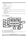

Chapter 23 Memory Mapping Control (S12XMMCV2)
MC9S12XDP512 Data Sheet, Rev. 2.11
Freescale Semiconductor 885
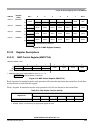
23.3.2 Register Descriptions
23.3.2.1 MMC Control Register (MMCCTL0)
Read: Anytime. In emulation modes read operations will return the data from the external bus. In all other
modes the data is read from this register.
Write: Anytime. In emulation modes write operations will also be directed to the external bus.
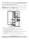
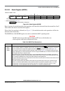
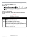
0x011C RAMWPC R
RPWE
00000
AVIE AVIF
W
0x011D RAMXGU R 1
XGU6 XGU5 XGU4 XGU3 XGU2 XGU1 XGU0
W
0x011E RAMSHL R 1
SHL6 SHL5 SHL4 SHL3 SHL2 SHL1 SHL0
W
0x011F RAMSHU R 1
SHU6 SHU5 SHU4 SHU3 SHU2 SHU1 SHU0
W
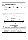
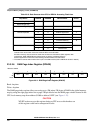
Address: 0x000A PRR
76543210
R0000
CS3E CS2E CS1E CS0E
W
Reset 0000000ROMON
1
1. ROMON is bit[0] of the register MMCTL1 (see Figure 1-10)
= Unimplemented or Reserved
Figure 23-3. MMC Control Register (MMCCTL0)
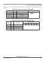
Table 23-3. Chip Selects Function Activity
Register Bit
Chip Modes
NS SS NX ES EX ST
CS3E, CS2E, CS1E, CS0E Disabled
1
1
Disabled: feature always inactive.
Disabled Enabled
2
2
Enabled: activity is controlled by the appropriate register bit value.
Disabled Enabled Enabled
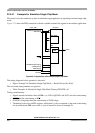
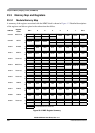
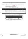
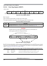
Address
Register
Name
Bit 7 654321Bit 0
= Unimplemented or Reserved
Figure 23-2. MMC Register Summary