


Chapter 19 Background Debug Module (S12XBDMV2)
MC9S12XDP512 Data Sheet, Rev. 2.11
Freescale Semiconductor 773
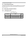
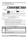
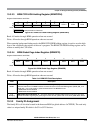
19.3.2.3 BDM CCR HIGH Holding Register (BDMCCRH)
Figure 19-5. BDM CCR HIGH Holding Register (BDMCCRH)
Read: All modes through BDM operation when not secured
Write: All modes through BDM operation when not secured
When entering background debug mode, the BDM CCR HIGH holding register is used to save the high
byte of the condition code register of the user’s program. The BDM CCR HIGH holding register can be
written to modify the CCR value.
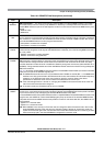
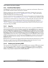
19.3.2.4 BDM Global Page Index Register (BDMGPR)
Figure 19-6. BDM Global Page Register (BDMGPR)
Read: All modes through BDM operation when not secured
Write: All modes through BDM operation when not secured
19.3.3 Family ID Assignment
The family ID is a 8-bit value located in the firmware ROM (at global address: 0x7FFF0F). The read-only
value is a unique family ID which is 0xC1 for S12X devices.
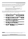
Register Global Address 0x7FFF07
7 6 5 4 3 2 1 0
R 0 0 0 0 0
CCR10 CCR9 CCR8
W
Reset 0 0 0 0 0 0 0 0
= Unimplemented or Reserved
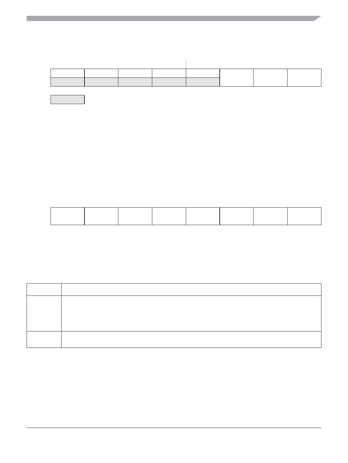
Register Global Address 0x7FFF08
7 6 5 4 3 2 1 0
R
BGAE BGP6 BGP5 BGP4 BGP3 BGP2 BGP1 BGP0
W
Reset 0 0 0 0 0 0 0 0
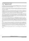
Table 19-4. BDMGPR Field Descriptions
Field Description
7
BGAE
BDM Global Page Access Enable Bit — BGAE enables global page access for BDM hardware and firmware
read/write instructions The BDM hardware commands used to access the BDM registers (READ_BD_ and
WRITE_BD_) can not be used for global accesses even if the BGAE bit is set.
0 BDM Global Access disabled
1 BDM Global Access enabled
6–0
BGP[6:0]
BDM Global Page Index Bits 6–0 — These bits define the extended address bits from 22 to 16. For more
detailed information regarding the global page window scheme, please refer to the S12X_MMC Block Guide.