


Appendix A Electrical Characteristics
MC9S12XDP512 Data Sheet, Rev. 2.11
Freescale Semiconductor 923
A.1.7 Operating Conditions
This section describes the operating conditions of the device. Unless otherwise noted those conditions
apply to all the following data.
NOTE
Please refer to the temperature rating of the device (C, V, M) with regards to
the ambient temperature T
A
and the junction temperature T
J
. For power
dissipation calculations refer to Section A.1.8, “Power Dissipation and
Thermal Characteristics”.
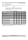
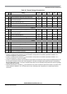
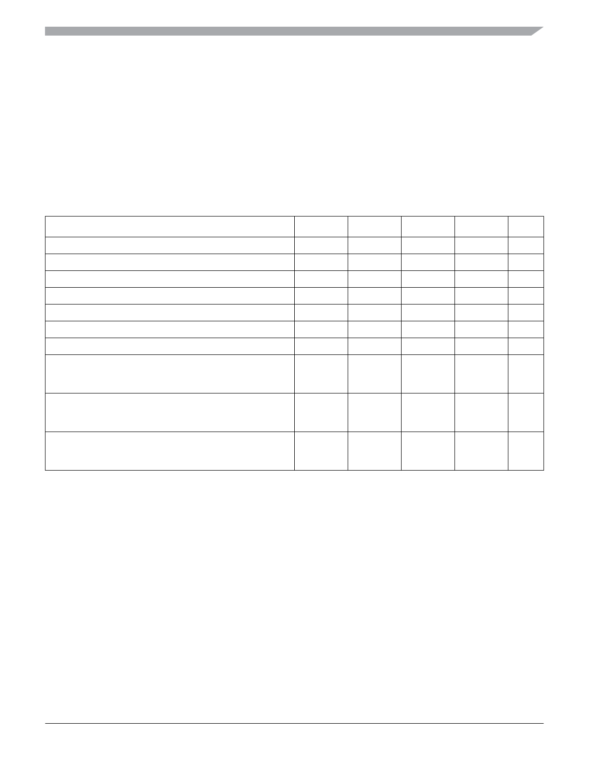
Table A-4. Operating Conditions
Rating Symbol Min Typ Max Unit
I/O, regulator and analog supply voltage V
DD35
3.15 5 5.5 V
Digital logic supply voltage
1
1
The device contains an internal voltage regulator to generate the logic and PLL supply out of the I/O supply. The absolute
maximum ratings apply when this regulator is disabled and the device is powered from an external source.
V
DD
2.35 2.5 2.75 V
PLL supply voltage
2
V
DDPLL
2.35 2.5 2.75 V
Voltage difference V
DDX
to V
DDR
and V
DDA
∆
VDDX
–0.1 0 0.1 V
Voltage difference V
SSX
to V
SSR
and V
SSA
∆
VSSX
–0.1 0 0.1 V
Oscillator f
osc
0.5 — 16 MHz
Bus frequency f
bus
0.5 — 40 MHz
MC9S12XDP512C
Operating junction temperature range
Operating ambient temperature range
2
2
Please refer to Section A.1.8, “Power Dissipation and Thermal Characteristics” for more details about the relation between
ambient temperature T
A
and device junction temperature T
J
.
T
J
T
A
–40
–40
—
27
100
85
°C
MC9S12XDP512V
Operating junction temperature range
Operating ambient temperature range
2
T
J
T
A
–40
–40
—
27
120
105
°C
MC9S12XDP512M
Operating junction temperature range
Operating ambient temperature range
2
T
J
T
A
–40
–40
—
27
140
125
°C