


Chapter 12 Pulse-Width Modulator (S12PWM8B8CV1)
MC9S12XDP512 Data Sheet, Rev. 2.11
582 Freescale Semiconductor
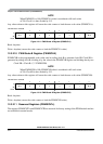
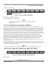
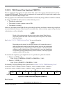
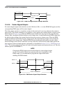
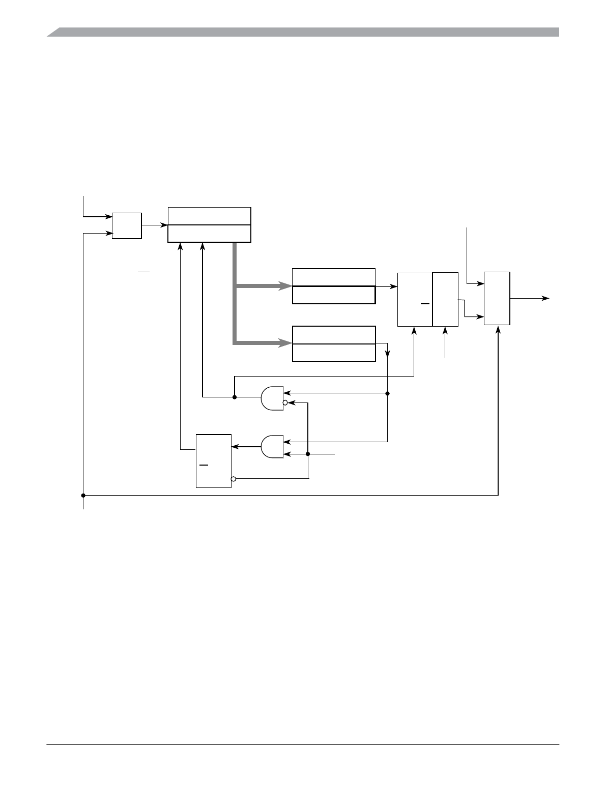
12.4.2 PWM Channel Timers
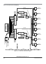
The main part of the PWM module are the actual timers. Each of the timer channels has a counter, a period
register and a duty register (each are 8-bit). The waveform output period is controlled by a match between
the period register and the value in the counter. The duty is controlled by a match between the duty register
and the counter value and causes the state of the output to change during the period. The starting polarity
of the output is also selectable on a per channel basis. Shown below in Figure 12-19 is the block diagram
for the PWM timer.
Figure 12-19. PWM Timer Channel Block Diagram
12.4.2.1 PWM Enable
Each PWM channel has an enable bit (PWMEx) to start its waveform output. When any of the PWMEx
bits are set (PWMEx = 1), the associated PWM output signal is enabled immediately. However, the actual
PWM waveform is not available on the associated PWM output until its clock source begins its next cycle
due to the synchronization of PWMEx and the clock source. An exception to this is when channels are
concatenated. Refer to Section 12.4.2.7, “PWM 16-Bit Functions” for more detail.
NOTE
The first PWM cycle after enabling the channel can be irregular.
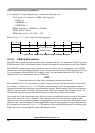
Clock Source
T
R
Q
Q
PPOLx
From Port PWMP
Data Register
PWMEx
To Pin
Driver
Gate
8-bit Compare =
PWMDTYx
8-bit Compare =
PWMPERx
CAEx
T
R
Q
Q
8-Bit Counter
PWMCNTx
M
U
X
M
U
X
(Clock Edge
Sync)
Up/Down Reset