


Appendix A Electrical Characteristics
MC9S12XDP512 Data Sheet, Rev. 2.11
924 Freescale Semiconductor
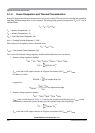
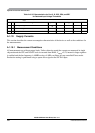
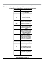
A.1.8 Power Dissipation and Thermal Characteristics
Power dissipation and thermal characteristics are closely related. The user must assure that the maximum
operating junction temperature is not exceeded. The average chip-junction temperature (T
J
) in °C can be
obtained from:
The total power dissipation can be calculated from:
Two cases with internal voltage regulator enabled and disabled must be considered:
1. Internal voltage regulator disabled
P
IO
is the sum of all output currents on I/O ports associated with V
DDX
and V
DDR
.
For R
DSON
is valid:
respectively
2. Internal voltage regulator enabled
I
DDR
is the current shown in Table A-10 and not the overall current flowing into V
DDR
, which
additionally contains the current flowing into the external loads with output high.
P
IO
is the sum of all output currents on I/O ports associated with V
DDX
and V
DDR
.
T
J
T
A
P
D
Θ
JA
•()+=
T
J
Junction Temperature, [°C]=
T
A
Ambient Temperature, [°C]=
P
D
Total Chip Power Dissipation, [W]=
Θ
JA
Package Thermal Resistance, [°C/W]=
P
D
P
INT
P
IO
+=
P
INT
Chip Internal Power Dissipation, [W]=
P
INT
I
DD
V
DD
⋅ I
DDPLL
V
DDPLL
⋅ I
DDA
+V
DDA
⋅+=
P
IO
R
DSON
i
∑
I
IO
i
2
⋅=
R
DSON
V
OL
I
OL
------------ for outputs driven low;=
R
DSON
V
DD5
V
OH
–
I
OH
------------------------------------ for outputs driven high;=
P
INT
I
DDR
V
DDR
⋅ I
DDA
V
DDA
⋅+=
P
IO
R
DSON
i
∑
I
IO
i
2
⋅=