


Chapter 11 Enhanced Capture Timer (S12MC9S12XDP51216B8CV2)
MC9S12XDP512 Data Sheet, Rev. 2.11
538 Freescale Semiconductor
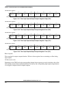
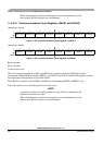
11.3.2.22 Delay Counter Control Register (DLYCT)
Read: Anytime
Write: Anytime
All bits reset to zero.
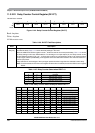
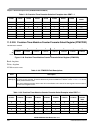
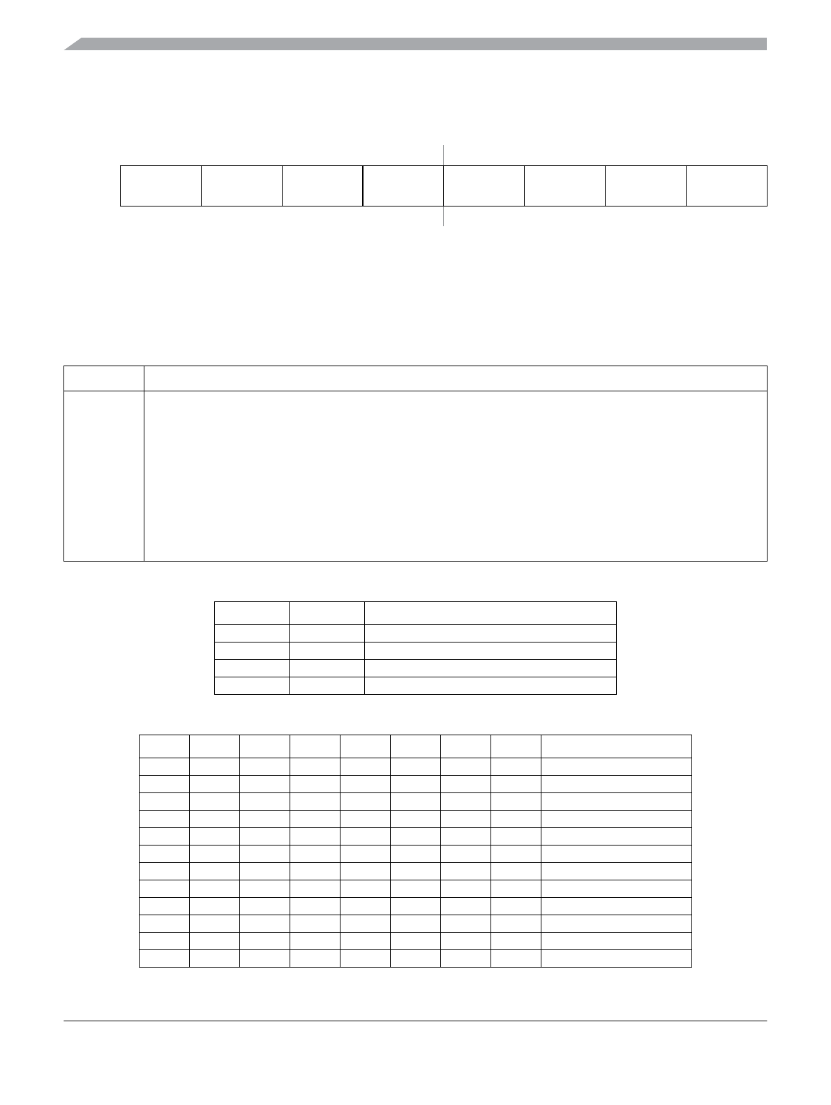
Module Base + 0x0029
76543210
R
DLY7 DLY6 DLY5 DLY4 DLY3 DLY2 DLY1 DLY0
W
Reset 00000000
Figure 11-44. Delay Counter Control Register (DLYCT)
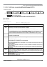
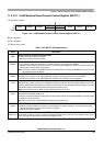
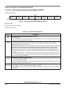
Table 11-26. DLYCT Field Descriptions
Field Description
7:0
DLY[7:0]
Delay Counter Select — When the PRNT bit of TSCR1 register is set to 0, only bits DLY0, DLY1 are used to
calculate the delay.Table 11-27 shows the delay settings in this case.
When the PRNT bit of TSCR1 register is set to 1, all bits are used to set a more precise delay. Table 11-28 shows
the delay settings in this case. After detection of a valid edge on an input capture pin, the delay counter counts
the pre-selected number of [(dly_cnt + 1)*4]bus clock cycles, then it will generate a pulse on its output if the level
of input signal, after the preset delay, is the opposite of the level before the transition.This will avoid reaction to
narrow input pulses.
Delay between two active edges of the input signal period should be longer than the selected counter delay.
Note: It is recommended to not write to this register while the timer is enabled, that is when TEN is set in register
TSCR1.
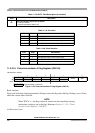
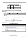
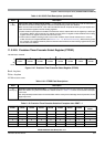
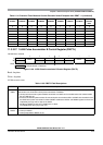
Table 11-27. Delay Counter Select when PRNT = 0
DLY1 DLY0 Delay
0 0 Disabled
0 1 256 bus clock cycles
1 0 512 bus clock cycles
1 1 1024 bus clock cycles
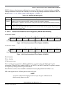
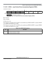
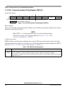
Table 11-28. Delay Counter Select Examples when PRNT = 1
DLY7 DLY6 DLY5 DLY4 DLY3 DLY2 DLY1 DLY0 Delay
00000000Disabled (bypassed)
00000001 8 bus clock cycles
0000001012 bus clock cycles
0000001116 bus clock cycles
0000010020 bus clock cycles
0000010124 bus clock cycles
0000011028 bus clock cycles
0000011132 bus clock cycles
0000111164 bus clock cycles
00011111128 bus clock cycles
00111111256 bus clock cycles
01111111512 bus clock cycles