


Chapter 9 XGATE (S12XGATEV2)
MC9S12XDP512 Data Sheet, Rev. 2.11
Freescale Semiconductor 375
9.3 Memory Map and Register Definition
This section provides a detailed description of address space and registers used by the XGATE module.
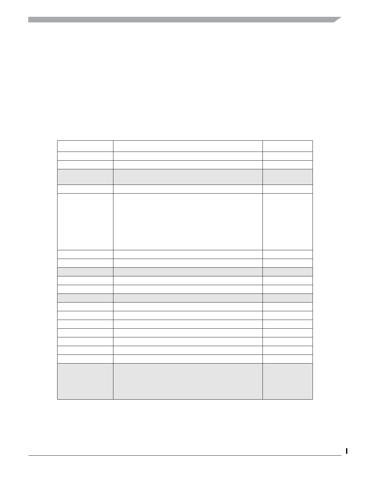
The memory map for the XGATE module is given below in Table 9-1.The address listed for each register
is the sum of a base address and an address offset. The base address is defined at the SoC level and the
address offset is defined at the module level. Reserved registers read zero. Write accesses to the reserved
registers have no effect.
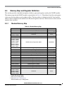
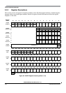
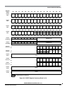
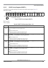
9.3.1 Module Memory Map
Table 9-1. Module Memory Map
Address Offset Use Access
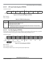
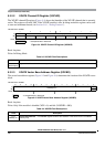
0x0000, 0x0001 XGATE Module Control Register (XGMCTL) Read/Write
1
1
Certain bits are not writable.
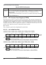
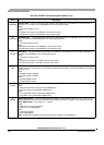
0x0002 XGATE Channel ID Register (XGCHID) Read/Write
1,2
2
Write only if in Debug Mode.
0x0003
0x0004, 0x0005
Reserved None
0x0006, 0x0007 XGATE Vector Base Address (XGVBR) Read/Write
1
0x0008, 0x0009,
0x000A, 0x000B,
0x000C, 0x000D,
0x000E, 0x000F,
0x0010, 0x0011,
0x0012, 0x0013,
0x0014, 0x0015,
0x0016, 0x0017
XGATE Interrupt Flag Vector (XGIF) Read/Write
1
0x0018, 0x0019 XGATE Software Trigger Register (XGSWT) Read/Write
0x001A, 0x001B XGATE Semaphore Register (XGSEM) Read/Write
3
3
See Section 9.4.4, “Semaphores”
0x001C Reserved None
0x001D XGATE Condition Code Register (XGCCR) Read/Write
1,4
4
Read and Write only if in Debug Mode.
0x001E, 0x001F XGATE Program Counter (XGPC) Read/Write
4
0x0020, 0x0021 Reserved None
0x0022, 0x0023 XGATE Register 1 (XGR1) Read/Write
4
0x0024, 0x0025 XGATE Register 2 (XGR2) Read/Write
4
0x0026, 0x0027 XGATE Register 3 (XGR3) Read/Write
4
0x0028, 0x0029 XGATE Register 4 (XGR4) Read/Write
4
0x002A,0x002B XGATE Register 5 (XGR5) Read/Write
4
0x002C, 0x002D XGATE Register 6 (XGR6) Read/Write
4
0x002E, 0x002F XGATE Register 7 (XGR7) Read/Write
4
0x0030, 0x0031,
0x0032, 0x0033,
0x0034, 0x0035,
0x0036, 0x0037,
0x0038, 0x0039
Reserved None