


Chapter 18 Periodic Interrupt Timer (S12PIT24B4CV1)
MC9S12XDP512 Data Sheet, Rev. 2.11
Freescale Semiconductor 751
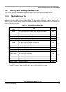
18.3 Memory Map and Register Definition
This section provides a detailed description of address space and registers used by the PIT.
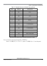
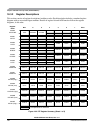
18.3.1 Module Memory Map
The memory map for the MC9S12XDP512 is given below in Table 1-1. The address listed for each register
is the sum of a base address and an address offset. The base address is defined at the SoC level and the
address offset is defined at the module level. Reads from the reserved bits return zeros and writes to the
reserved bits have no effect.
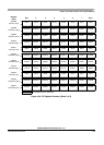
Table 18-1. MC9S12XDP512 Memory Map
Address
Offset
Use Access
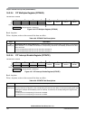
0x0000 PIT Control and Force Load Micro Timer Register (PITCFLMT) R/W
1
1
Certain bits are non-writable.
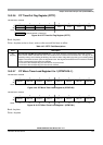
0x0001 PIT Force Load Timer Register (PITFLT) R/W
1,2
2
Reading from this register returns all zeros.
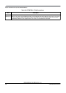
0x0002 PIT Channel Enable Register (PITCE) R/W
1
0x0003 PIT Multiplex Register (PITMUX) R/W
1
0x0004 PIT Interrupt Enable Register (PITINTE) R/W
1
0x0005 PIT Time-Out Flag Register (PITTF) R/W
1
0x0006 PIT Micro Timer Load Register 0 (PITMTLD0) R/W
0x0007 PIT Micro Timer Load Register 1 (PITMTLD1) R/W
0x0008, 0x0009 PIT Load Register 0 (PITLD0) R/W
0x000A, 0x000B PIT Count Register 0 (PITCNT0) R/W
0x000C, 0x000D PIT Load Register 1 (PITLD1) R/W
0x000E, 0x000F PIT Count Register 1 (PITCNT1) R/W
0x0010, 0x0011 PIT Load Register 2 (PITLD2) R/W
0x0012, 0x0013 PIT Count Register 2 (PITCNT2) R/W
0x0014, 0x0015 PIT Load Register 3 (PITLD3) R/W
0x0016, 0x0017 PIT Count Register 3 (PITCNT3) R/W
0x0018 - 0x0027 Reserved Registers
3
3
Reading from these registers returns all zeros. Writing to these registers has no effect.
R/W