


Chapter 4 Port Integration Module (S12XDP512PIMV2)
MC9S12XDP512 Data Sheet, Rev. 2.11
Freescale Semiconductor 261
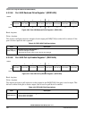
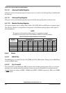
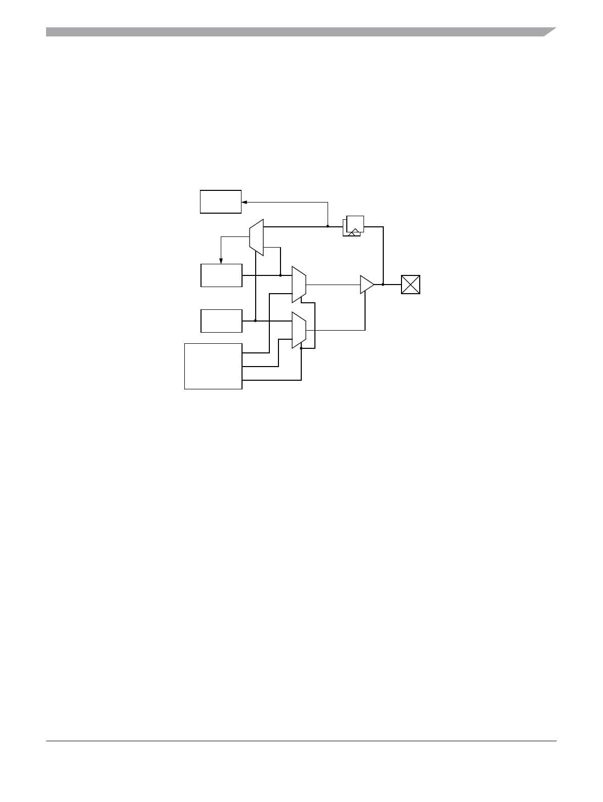
4.4.1.2 Input Register
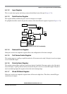
This is a read-only register and always returns the buffered state of the pin (Figure 4-76).
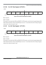
4.4.1.3 Data Direction Register
This register defines whether the pin is used as an input or an output.
If a peripheral module controls the pin the contents of the data direction register is ignored (Figure 4-76).
Figure 4-76. Illustration of I/O Pin Functionality
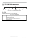
4.4.1.4 Reduced Drive Register
If the pin is used as an output this register allows the configuration of the drive strength.
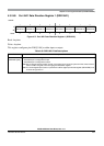
4.4.1.5 Pull Device Enable Register
This register turns on a pull-up or pull-down device. It becomes active only if the pin is used as an input
or as a wired-OR output.
4.4.1.6 Polarity Select Register
This register selects either a pull-up or pull-down device if enabled. It becomes active only if the pin is
used as an input. A pull-up device can be activated if the pin is used as a wired-OR output. If the pin is
used as an interrupt input this register selects the active interrupt edge.
4.4.1.7 Wired-OR Mode Register
If the pin is used as an output this register turns off the active high drive. This allows wired-OR type
connections of outputs.
PT
DDR
output enable
module enable
1
0
1
1
0
0
PIN
PTI
data out
Module