


Appendix A Electrical Characteristics
MC9S12XDP512 Data Sheet, Rev. 2.11
944 Freescale Semiconductor
A.5 Reset, Oscillator, and PLL
This section summarizes the electrical characteristics of the various startup scenarios for oscillator and
phase-locked loop (PLL).
A.5.1 Startup
Table A-20 summarizes several startup characteristics explained in this section. Detailed description of the
startup behavior can be found in the Clock and Reset Generator (CRG) Block Guide.
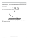
A.5.1.1 POR
The release level V
PORR
and the assert level V
PORA
are derived from the V
DD
supply. They are also valid
if the device is powered externally. After releasing the POR reset the oscillator and the clock quality check
are started. If after a time t
CQOUT
no valid oscillation is detected, the MCU will start using the internal self
clock. The fastest startup time possible is given by n
uposc
.
A.5.1.2 SRAM Data Retention
Provided an appropriate external reset signal is applied to the MCU, preventing the CPU from executing
code when V
DD35
is out of specification limits, the SRAM contents integrity is guaranteed if after the reset
the PORF bit in the CRG flags register has not been set.
A.5.1.3 External Reset
When external reset is asserted for a time greater than PW
RSTL
the CRG module generates an internal
reset, and the CPU starts fetching the reset vector without doing a clock quality check, if there was an
oscillation before reset.
A.5.1.4 Stop Recovery
Out of stop the controller can be woken up by an external interrupt. A clock quality check as after POR is
performed before releasing the clocks to the system.
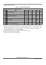
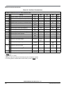
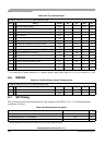
Table A-20. Startup Characteristics
Conditions are shown in Table A-4unless otherwise noted
Num C Rating Symbol Min Typ Max Unit
1 D Reset input pulse width, minimum input time PW
RSTL
2——t
osc
2 D Startup from reset n
RST
192 — 196 n
osc
3 D Interrupt pulse width, IRQ edge-sensitive mode PW
IRQ
20 — — ns
4 D Wait recovery startup time t
WRS
— — 14 t
cyc
5 D Fast wakeup from STOP
1
1
V
DD1
/V
DD2
filter capacitors 220 nF, V
DD35
= 5 V, T= 25°C
t
fws
—50—µs