


Chapter 1 Device Overview (MC9S12XDP512V2)
MC9S12XDP512 Data Sheet, Rev. 2.11
92 Freescale Semiconductor
The program Flash memory and the EEPROM are supplied by the bus clock and the oscillator clock.The
oscillator clock is used as a time base to derive the program and erase times for the NVM’s. Consult the
FTX512k4 Block Guide and the EETX4K Block Guide for more details on the operation of the NVM’s.
The CAN modules may be configured to have their clock sources derived either from the bus clock or
directly from the oscillator clock. This allows the user to select its clock based on the required jitter
performance. Consult MSCAN block description for more details on the operation and configuration of
the CAN blocks.
In order to ensure the presence of the clock the MCU includes an on-chip clock monitor connected to the
output of the oscillator. The clock monitor can be configured to invoke the PLL self-clocking mode or to
generate a system reset if it is allowed to time out as a result of no oscillator clock being present.
In addition to the clock monitor, the MCU also provides a clock quality checker which performs a more
accurate check of the clock. The clock quality checker counts a predetermined number of clock edges
within a defined time window to insure that the clock is running. The checker can be invoked following
specific events such as on wake-up or clock monitor failure.
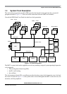
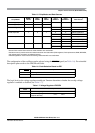
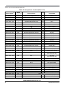
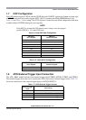
1.4 Chip Configuration Summary
The MCU can operate in six different modes. The different modes, the state of ROMCTL and EROMCTL
signal on rising edge of
RESET, and the security state of the MCU affects the following device
characteristics:
• External bus interface configuration
• Flash in memory map, or not
• Debug features enabled or disabled
The operating mode out of reset is determined by the states of the MODC, MODB, and MODA signals
during reset (see Table 1-5). The MODC, MODB, and MODA bits in the MODE register show the current
operating mode and provide limited mode switching during operation. The states of the MODC, MODB,
and MODA signals are latched into these bits on the rising edge of
RESET.
In normal expanded mode and in emulation modes the ROMON bit and the EROMON bit in the
MMCCTL1 register defines if the on chip flash memory is the memory map, or not. (See Table 1-5.) For
a detailed description of the ROMON and EROMON bits refer to the S12X_MMC Block Guide.
The state of the ROMCTL signal is latched into the ROMON bit in the MMCCTL1 register on the rising
edge of
RESET. The state of the EROMCTL signal is latched into the EROMON bit in the MISC register
on the rising edge of
RESET.