


MC9S12XDP512 Data Sheet, Rev. 2.11
Freescale Semiconductor 881
Chapter 23
Memory Mapping Control (S12XMMCV2)
23.1 Introduction
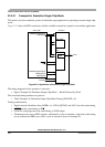
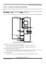
This section describes the functionality of the module mapping control (MMC) sub-block of the S12X
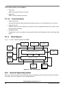
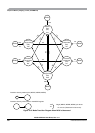
platform. The block diagram of the MMC is shown in Figure 1-1.
The MMC module controls the multi-master priority accesses, the selection of internal resources and
external space. Internal buses including internal memories and peripherals are controlled in this module.
The local address space for each master is translated to a global memory space.
23.1.1 Features
The main features of this block are:
• Paging capability to support a global 8 Mbytes memory address space
• Bus arbitration between the masters CPU, BDM, and XGATE
• Simultaneous accesses to different resources
1
(internal, external, and peripherals) (see Figure 1-1)
• Resolution of target bus access collision
• Access restriction control from masters to some targets (e.g., RAM write access protection for user
specified areas)
• MCU operation mode control
• MCU security control
• Separate memory map schemes for each master CPU, BDM, and XGATE
• ROM control bits to enable the on-chip FLASH or ROM selection
• Port replacement registers access control
• Generation of system reset when CPU accesses an unimplemented address (i.e., an address which
does not belong to any of the on-chip modules) in single-chip modes
23.1.2 Modes of Operation
This subsection lists and briefly describes all operating modes supported by the MMC.
23.1.2.1 Power Saving Modes
• Run mode
MMC is functional during normal run mode.
1. Resources are also called targets.