


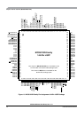
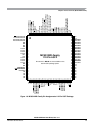
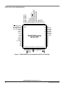
Chapter 1 Device Overview (MC9S12XDP512V2)
MC9S12XDP512 Data Sheet, Rev. 2.11
Freescale Semiconductor 79
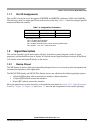
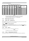
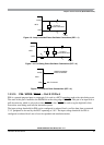
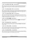
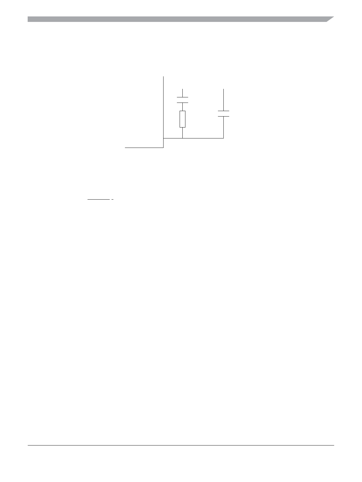
1.2.3.5 XFC — PLL Loop Filter Pin
Please ask your Freescale representative for the interactive application note to compute PLL loop filter
elements. Any current leakage on this pin must be avoided.
Figure 1-8. PLL Loop Filter Connections
1.2.3.6 BKGD / MODC — Background Debug and Mode Pin
The BKGD/MODC pin is used as a pseudo-open-drain pin for the background debug communication. It
is used as a MCU operating mode select pin during reset. The state of this pin is latched to the MODC bit
at the rising edge of
RESET. The BKGD pin has a pullup device.
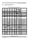
1.2.3.7 PAD[23:8] / AN[23:8] — Port AD Input Pins of ATD1
PAD[23:8] are general-purpose input or output pins and analog inputs AN[23:8] of the analog-to-digital
converter ATD1.
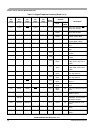
1.2.3.8 PAD[7:0] / AN[7:0] — Port AD Input Pins of ATD0
PAD[7:0] are general-purpose input or output pins and analog inputs AN[7:0] of the analog-to-digital
converter ATD0.
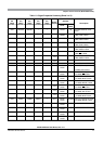
1.2.3.9 PA[7:0] / ADDR[15:8] / IVD[15:8] — Port A I/O Pins
PA[7:0] are general-purpose input or output pins. In MCU expanded modes of operation, these pins are
used for the external address bus. In MCU emulation modes of operation, these pins are used for external
address bus and internal visibility read data.
1.2.3.10 PB[7:1] / ADDR[7:1] / IVD[7:1] — Port B I/O Pins
PB[7:1] are general-purpose input or output pins. In MCU expanded modes of operation, these pins are
used for the external address bus. In MCU emulation modes of operation, these pins are used for external
address bus and internal visibility read data.
MCU
XFC
R
0
C
S
C
P
V
DDPLL
V
DDPLL