


Chapter 10 Security (S12X9SECV2)
MC9S12XDP512 Data Sheet, Rev. 2.11
500 Freescale Semiconductor
10.1.2 Modes of Operation
10.1.3 Securing the Microcontroller
Once the user has programmed the Flash and EEPROM, the chip can be secured by programming the
security bits located in the options/security byte in the Flash memory array. These non-volatile bits will
keep the device secured through reset and power-down.
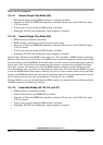
The options/security byte is located at address 0xFF0F (= global address 0x7F_FF0F) in the Flash memory
array. This byte can be erased and programmed like any other Flash location. Two bits of this byte are used
for security (SEC[1:0]). On devices which have a memory page window, the Flash options/security byte
is also available at address 0xBF0F by selecting page 0x3F with the PPAGE register. The contents of this
byte are copied into the Flash security register (FSEC) during a reset sequence.
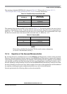
Table 10-1. Features Availability in Unsecure and Secure Modes
Unsecure Mode Secure Mode
NS SS NX ES EX ST NS SS NX ES EX ST
Flash Array Access ✔✔✔
1
1
Availability of Flash arrays in the memory map depends on ROMCTL/EROMCTL pins and/or the state of
the ROMON/EROMON bits in the MMCCTL1 register. Please refer to the S12X_MMC block guide for
detailed information.
✔
1
✔
1
✔
1
✔✔————
EEPROM Array Access ✔✔✔✔✔✔✔✔————
NVM Commands ✔
2
2
Restricted NVM command set only. Please refer to the FTX/EETX block guides for detailed information.
✔✔
2
✔
2
✔
2
✔✔
2
✔
2
✔
2
✔
2
✔
2
✔
2
BDM ✔✔✔✔✔✔— ✔
3
3
BDM hardware commands restricted to peripheral registers only.
————
DBG Module Trace ✔✔✔✔✔✔——————
XGATE Debugging ✔✔✔✔✔✔——————
External Bus Interface — — ✔✔✔✔——✔✔✔✔
Internal status visible
multiplexed on
external bus
———✔✔————✔✔—
Internal accesses visible
on external bus
—————✔ —————✔
76543210
0xFF0F KEYEN1 KEYEN0 NV5 NV4 NV3 NV2 SEC1 SEC0
Figure 10-1. Flash Options/Security Byte