


Appendix A Electrical Characteristics
MC9S12XDP512 Data Sheet, Rev. 2.11
Freescale Semiconductor 953
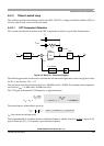
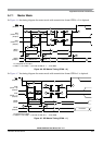
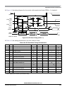
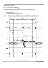
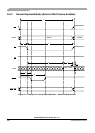
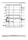
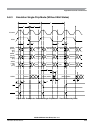
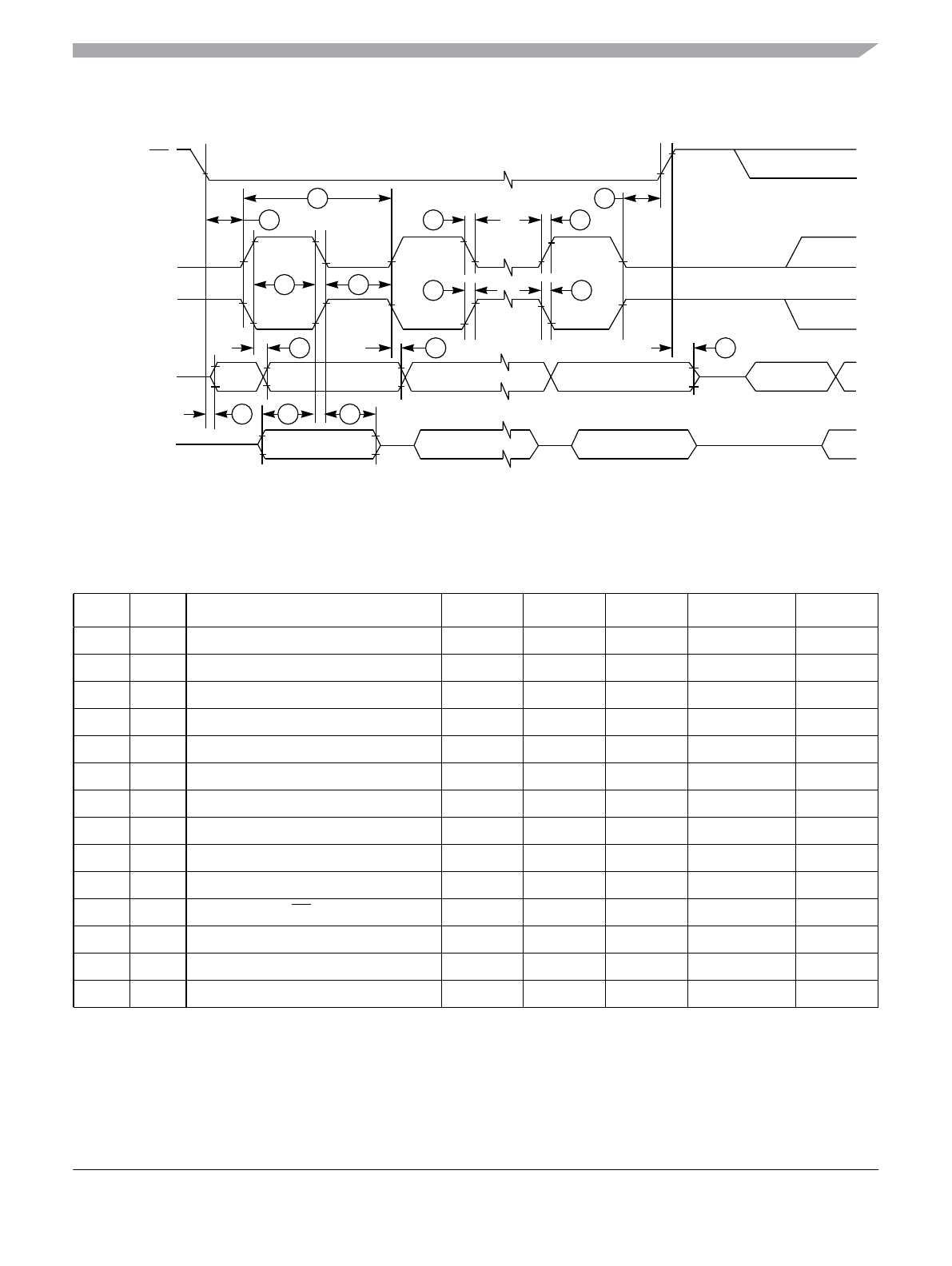
In Figure A-9 the timing diagram for slave mode with transmission format CPHA = 1 is depicted.
Figure A-9. SPI Slave Timing (CPHA = 1)
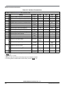
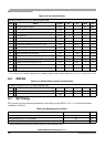
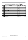
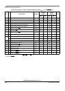
In Table A-26 the timing characteristics for slave mode are listed.
Table A-26. SPI Slave Mode Timing Characteristics
Num C Characteristic Symbol Min Typ Max Unit
1 D SCK frequency f
sck
DC — 1/4f
bus
1 D SCK period t
sck
4— ∞ t
bus
2 D Enable lead time t
lead
4— — t
bus
3 D Enable lag time t
lag
4— — t
bus
4 D Clock (SCK) high or low time t
wsck
4— — t
bus
5 D Data setup time (inputs) t
su
8— — ns
6 D Data hold time (inputs) t
hi
8— — ns
7 D Slave access time (time to data active) t
a
— — 20 ns
8 D Slave MISO disable time t
dis
— — 22 ns
9 D Data valid after SCK edge t
vsck
— — 29 + 0.5 ⋅ t
bus
1
1
0.5 t
bus
added due to internal synchronization delay
ns
10 D Data valid after SS fall t
vss
— — 29 + 0.5 ⋅ t
bus
1
ns
11 D Data hold time (outputs) t
ho
20 — — ns
12 D Rise and fall time inputs t
rfi
—— 8 ns
13 D Rise and fall time outputs t
rfo
—— 8 ns
SCK
(Input)
SCK
(Input)
MOSI
(Input)
MISO
(Output)
1
5 6
MSB IN
Bit 6 . . . 1
LSB IN
MSB OUT Slave LSB OUT
Bit 6 . . . 1
4
4
9
12 13
11
(CPOL = 0)
(CPOL = 1)
SS
(Input)
2
12 13
3
NOTE: Not defined
Slave
7
8
See
Note