


Chapter 16 Serial Peripheral Interface (S12SPIV4)
MC9S12XDP512 Data Sheet, Rev. 2.11
Freescale Semiconductor 715
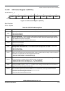
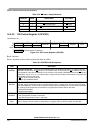
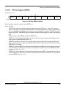
16.3.2.1 SPI Control Register 1 (SPICR1)
Read: Anytime
Write: Anytime
Module Base +0x___0
76543210
R
SPIE SPE SPTIE MSTR CPOL CPHA SSOE LSBFE
W
Reset 00000100
Figure 16-3. SPI Control Register 1 (SPICR1)
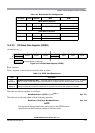
Table 16-2. SPICR1 Field Descriptions
Field Description
7
SPIE
SPI Interrupt Enable Bit — This bit enables SPI interrupt requests, if SPIF or MODF status flag is set.
0 SPI interrupts disabled.
1 SPI interrupts enabled.
6
SPE
SPI System Enable Bit — This bit enables the SPI system and dedicates the SPI port pins to SPI system
functions. If SPE is cleared, SPI is disabled and forced into idle state, status bits in SPISR register are reset.
0 SPI disabled (lower power consumption).
1 SPI enabled, port pins are dedicated to SPI functions.
5
SPTIE
SPI Transmit Interrupt Enable — This bit enables SPI interrupt requests, if SPTEF flag is set.
0 SPTEF interrupt disabled.
1 SPTEF interrupt enabled.
4
MSTR
SPI Master/Slave Mode Select Bit — This bit selects whether the SPI operates in master or slave mode.
Switching the SPI from master to slave or vice versa forces the SPI system into idle state.
0 SPI is in slave mode.
1 SPI is in master mode.
3
CPOL
SPI Clock Polarity Bit — This bit selects an inverted or non-inverted SPI clock. To transmit data between SPI
modules, the SPI modules must have identical CPOL values. In master mode, a change of this bit will abort a
transmission in progress and force the SPI system into idle state.
0 Active-high clocks selected. In idle state SCK is low.
1 Active-low clocks selected. In idle state SCK is high.
2
CPHA
SPI Clock Phase Bit — This bit is used to select the SPI clock format. In master mode, a change of this bit will
abort a transmission in progress and force the SPI system into idle state.
0 Sampling of data occurs at odd edges (1,3,5,...,15) of the SCK clock.
1 Sampling of data occurs at even edges (2,4,6,...,16) of the SCK clock.
1
SSOE
Slave Select Output Enable — The
SS output feature is enabled only in master mode, if MODFEN is set, by
asserting the SSOE as shown in Table 16-3. In master mode, a change of this bit will abort a transmission in
progress and force the SPI system into idle state.
0
LSBFE
LSB-First Enable — This bit does not affect the position of the MSB and LSB in the data register. Reads and
writes of the data register always have the MSB in bit 7. In master mode, a change of this bit will abort a
transmission in progress and force the SPI system into idle state.
0 Data is transferred most significant bit first.
1 Data is transferred least significant bit first.