


Chapter 5 Clocks and Reset Generator (S12CRGV6)
MC9S12XDP512 Data Sheet, Rev. 2.11
290 Freescale Semiconductor
5.4 Functional Description
5.4.1 Functional Blocks
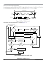
5.4.1.1 Phase Locked Loop (PLL)
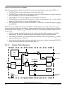
The PLL is used to run the MCU from a different time base than the incoming OSCCLK. For increased
flexibility, OSCCLK can be divided in a range of 1 to 16 to generate the reference frequency. This offers
a finer multiplication granularity. The PLL can multiply this reference clock by a multiple of 2, 4, 6,...
126,128 based on the SYNR register.
CAUTION
Although it is possible to set the two dividers to command a very high clock
frequency, do not exceed the specified bus frequency limit for the MCU.
If (PLLSEL = 1), Bus Clock = PLLCLK / 2
The PLL is a frequency generator that operates in either acquisition mode or tracking mode, depending on
the difference between the output frequency and the target frequency. The PLL can change between
acquisition and tracking modes either automatically or manually.
The VCO has a minimum operating frequency, which corresponds to the self clock mode frequency f
SCM
.
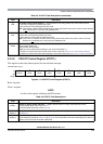
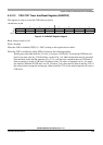
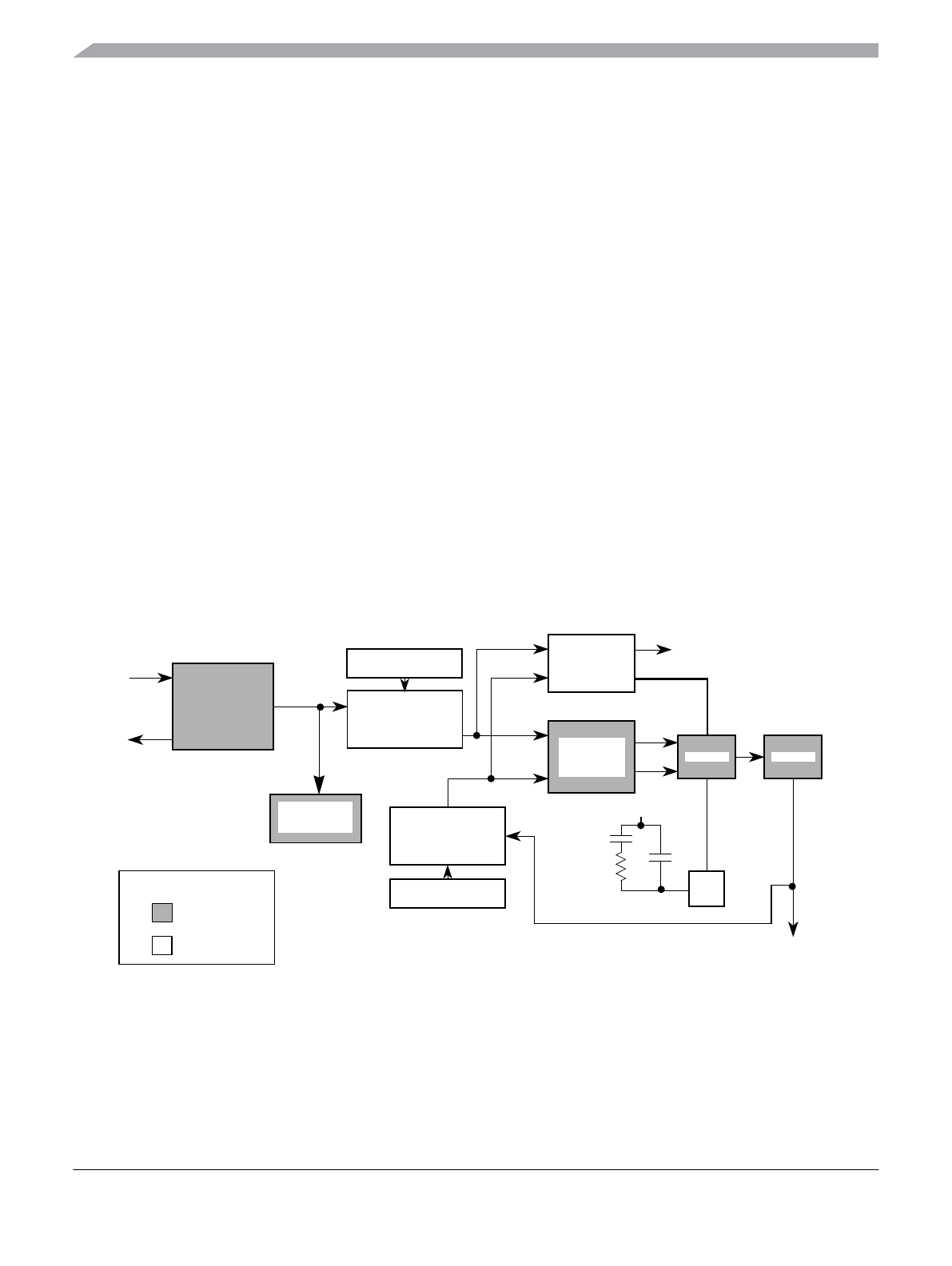
Figure 5-16. PLL Functional Diagram
PLLCLK 2 OSCCLK
SYNR 1+[]
REFDV 1+[]
------------------------------------
××=
REDUCED
CONSUMPTION
OSCILLATOR
EXTAL
XTAL
OSCCLK
PLLCLK
REFERENCE
PROGRAMMABLE
DIVIDER
PDET
PHASE
DETECTOR
REFDV <5:0>
LOOP
PROGRAMMABLE
DIVIDER
SYN <5:0>
CPUMP VCO
LOCK
LOOP
FILTER
XFC
PIN
UP
DOWN
LOCK
DETECTOR
REFERENCE
FEEDBACK
V
DDPLL
V
DDPLL
/V
SSPLL
CRYSTAL
MONITOR
V
DDPLL
/V
SSPLL
V
DD
/V
SS
supplied by: