


MC9S12XDP512 Data Sheet, Rev. 2.11
Freescale Semiconductor 765
Chapter 19
Background Debug Module (S12XBDMV2)
19.1 Introduction
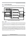
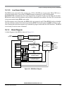
This section describes the functionality of the background debug module (BDM) sub-block of the
HCS12X core platform.
The background debug module (BDM) sub-block is a single-wire, background debug system implemented
in on-chip hardware for minimal CPU intervention. All interfacing with the BDM is done via the BKGD
pin.
The BDM has enhanced capability for maintaining synchronization between the target and host while
allowing more flexibility in clock rates. This includes a sync signal to determine the communication rate
and a handshake signal to indicate when an operation is complete. The system is backwards compatible to
the BDM of the S12 family with the following exceptions:
• TAGGO command no longer supported by BDM
• External instruction tagging feature now part of DBG module
• BDM register map and register content extended/modified
• Global page access functionality
• Enabled but not active out of reset in emulation modes
• CLKSW bit set out of reset in emulation mode.
• Family ID readable from firmware ROM at global address 0x7FFF0F (value for HCS12X devices
is 0xC1)
19.1.1 Features
The BDM includes these distinctive features:
• Single-wire communication with host development system
• Enhanced capability for allowing more flexibility in clock rates
• SYNC command to determine communication rate
• GO_UNTIL command
• Hardware handshake protocol to increase the performance of the serial communication
• Active out of reset in special single chip mode
• Nine hardware commands using free cycles, if available, for minimal CPU intervention
• Hardware commands not requiring active BDM
• 14 firmware commands execute from the standard BDM firmware lookup table