


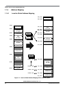

Chapter 1 Device Overview (MC9S12XDP512V2)
MC9S12XDP512 Data Sheet, Rev. 2.11
28 Freescale Semiconductor
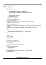
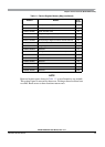
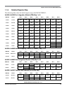
1.1.4 Device Memory Map
Table 1-1shows the device register memory map of the MC9S12XDP512.
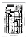
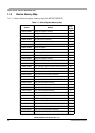
Table 1-1. Device Register Memory Map
Address Module
Size
(Bytes)
0x0000–0x0009 PIM (port integration module
) 10
0x000A–0x000B MMC (memory map control) 2
0x000C–0x000D PIM (port integration module) 2
0x000E–0x000F EBI (external bus interface) 2
0x0010–0x0017 MMC (memory map control) 8
0x0018–0x0019 Reserved 2
0x001A–0x001B Device ID register 2
0x001C–0x001F PIM (port integration module) 4
0x0020–0x002F DBG (debug module) 16
0x0030–0x0031 MMC (memory map control) 2
0x0032–0x0033 PIM (port integration module) 2
0x0034–0x003F CRG (clock and reset generator) 12
0x0040–0x007F ECT (enhanced capture timer 16-bit 8-channel)s 64
0x0080–0x00AF ATD1 (analog-to-digital converter 10-bit 16-channel) 48
0x00B0–0x00B7 IIC1 (inter IC bus) 8
0x00B8–0x00BF SCI2 (serial communications interface) 8
0x00C0–0x00C7 SCI3 (serial communications interface) 8
0x00C8–0x00CF SCI0 (serial communications interface) 8
0x00D0–0x00D7 SCI1 (serial communications interface) 8
0x00D8–0x00DF SPI0 (serial peripheral interface) 8
0x00E0–0x00E7 IIC0 (inter IC bus) 8
0x00E8–0x00EF Reserved 8
0x00F0–0x00F7 SPI1 (serial peripheral interface) 8
0x00F8–0x00FF SPI2 (serial peripheral interface) 8
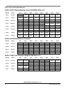
0x0100–0x010F Flash control register 16
0x0110–0x011B EEPROM control register 12
0x011C–0x011F MMC (memory map control) 4
0x0120–0x012F INT (interrupt module) 16
0x0130–0x0137 SCI4 (serial communications interface) 8
0x0138–0x013F SCI5 (serial communications interface) 8
0x0140–0x017F CAN0 (scalable CAN) 64