


Chapter 12 Pulse-Width Modulator (S12PWM8B8CV1)
MC9S12XDP512 Data Sheet, Rev. 2.11
Freescale Semiconductor 577
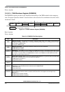
12.3.2.14 PWM Channel Duty Registers (PWMDTYx)
There is a dedicated duty register for each channel. The value in this register determines the duty of the
associated PWM channel. The duty value is compared to the counter and if it is equal to the counter value
a match occurs and the output changes state.
The duty registers for each channel are double buffered so that if they change while the channel is enabled,
the change will NOT take effect until one of the following occurs:
• The effective period ends
• The counter is written (counter resets to $00)
• The channel is disabled
In this way, the output of the PWM will always be either the old duty waveform or the new duty waveform,
not some variation in between. If the channel is not enabled, then writes to the duty register will go directly
to the latches as well as the buffer.
NOTE
Reads of this register return the most recent value written. Reads do not
necessarily return the value of the currently active duty due to the double
buffering scheme.
See Section 12.4.2.3, “PWM Period and Duty” for more information.
NOTE
Depending on the polarity bit, the duty registers will contain the count of
either the high time or the low time. If the polarity bit is one, the output starts
high and then goes low when the duty count is reached, so the duty registers
contain a count of the high time. If the polarity bit is zero, the output starts
low and then goes high when the duty count is reached, so the duty registers
contain a count of the low time.
To calculate the output duty cycle (high time as a% of period) for a particular channel:
• Polarity = 0 (PPOL x =0)
Duty Cycle = [(PWMPERx-PWMDTYx)/PWMPERx] * 100%
• Polarity = 1 (PPOLx = 1)
Duty Cycle = [PWMDTYx / PWMPERx] * 100%
For boundary case programming values, please refer to Section 12.4.2.8, “PWM Boundary Cases”.
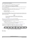
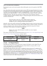
Read: Anytime
Module Base + 0x001C = PWMDTY0, 0x001D = PWMDTY1, 0x001E = PWMDTY2, 0x001F = PWMDTY3
Module Base + 0x0020 = PWMDTY4, 0x0021 = PWMDTY5, 0x0022 = PWMDTY6, 0x0023 = PWMDTY7
76543210
R
Bit 7 6 5 4 3 2 1 Bit 0
W
Reset 11111111
Figure 12-16. PWM Channel Duty Registers (PWMDTYx)