


Chapter 8 Analog-to-Digital Converter (ATD10B8CV3)
MC9S12XDP512 Data Sheet, Rev. 2.11
370 Freescale Semiconductor
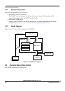
8.4.1.2 Analog Input Multiplexer
The analog input multiplexer connects one of the 8 external analog input channels to the sample and hold
machine.
8.4.1.3 Sample Buffer Amplifier
The sample amplifier is used to buffer the input analog signal so that the storage node can be quickly
charged to the sample potential.
8.4.1.4 Analog-to-Digital (A/D) Machine
The A/D Machine performs analog to digital conversions. The resolution is program selectable at either 8
or 10 bits. The A/D machine uses a successive approximation architecture. It functions by comparing the
stored analog sample potential with a series of digitally generated analog potentials. By following a binary
search algorithm, the A/D machine locates the approximating potential that is nearest to the sampled
potential.
When not converting the A/D machine disables its own clocks. The analog electronics still draws quiescent
current. The power down (ADPU) bit must be set to disable both the digital clocks and the analog power
consumption.
Only analog input signals within the potential range of V
RL
to V
RH
(A/D reference potentials) will result
in a non-railed digital output codes.
8.4.2 Digital Sub-Block
This subsection explains some of the digital features in more detail. See register descriptions for all details.
8.4.2.1 External Trigger Input
The external trigger feature allows the user to synchronize ATD conversions to the external environment
events rather than relying on software to signal the ATD module when ATD conversions are to take place.
The external trigger signal (out of reset ATD channel 7, configurable in ATDCTL1) is programmable to
be edge or level sensitive with polarity control. Table 8-23 gives a brief description of the different
combinations of control bits and their effect on the external trigger function.