


Chapter 7 Analog-to-Digital Converter (ATD10B16CV4)
MC9S12XDP512 Data Sheet, Rev. 2.11
Freescale Semiconductor 323
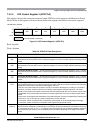
7.3.2.2 ATD Control Register 1 (ATDCTL1)
Writes to this register will abort current conversion sequence but will not start a new sequence.
Read: Anytime
Write: Anytime
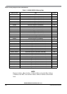
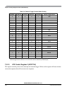
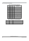
Table 7-3. Multi-Channel Wrap Around Coding
WRAP3 WRAP2 WRAP1 WRAP0
Multiple Channel Conversions
(MULT = 1) Wrap Around to AN0
after Converting
0 0 0 0 Reserved
0001 AN1
0010 AN2
0011 AN3
0100 AN4
0101 AN5
0110 AN6
0111 AN7
1000 AN8
1001 AN9
1 0 1 0 AN10
1 0 1 1 AN11
1 1 0 0 AN12
1 1 0 1 AN13
1 1 1 0 AN14
1 1 1 1 AN15
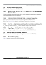
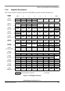
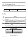
Module Base + 0x0001
76543210
R
ETRIGSEL
000
ETRIGCH3 ETRIGCH2 ETRIGCH1 ETRIGCH0
W
Reset 00001111
= Unimplemented or Reserved
Figure 7-4. ATD Control Register 1 (ATDCTL1)
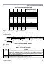
Table 7-4. ATDCTL1 Field Descriptions
Field Description
7
ETRIGSEL
External Trigger Source Select — This bit selects the external trigger source to be either one of the AD
channels or one of the ETRIG[3:0] inputs. See device specification for availability and connectivity of
ETRIG[3:0] inputs. If ETRIG[3:0] input option is not available, writing a 1 to ETRISEL only sets the bit but has
no effect, that means one of the AD channels (selected by ETRIGCH[3:0]) remains the source for external
trigger. The coding is summarized in Table 7-5.
3:0
ETRIGCH[3:0]
External Trigger Channel Select — These bits select one of the AD channels or one of the ETRIG[3:0] inputs
as source for the external trigger. The coding is summarized in Table 7-5.