


Chapter 1 Device Overview (MC9S12XDP512V2)
MC9S12XDP512 Data Sheet, Rev. 2.11
90 Freescale Semiconductor
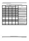
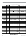
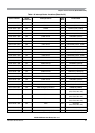
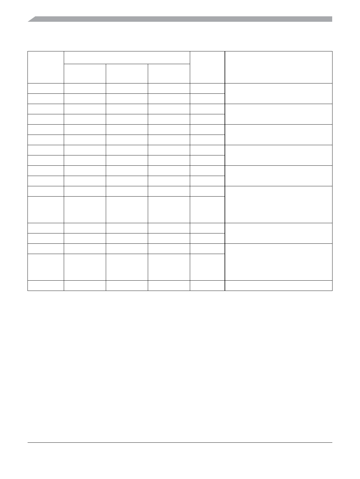
Table 1-4. MC9S12XDP512 Power and Ground Connection Summary
Mnemonic
Pin Number
Nominal
Voltage
Description
144-Pin
LQFP
112-Pin
LQFP
80-Pin
QFP
V
DD1, 2
15, 87 13, 65 9, 49 2.5 V Internal power and ground generated by
internal regulator
V
SS1, 2
16, 88 14, 66 10, 50 0V
V
DDR1
53 41 29 5.0 V External power and ground, supply to pin
drivers and internal voltage regulator
V
SSR1
52 40 28 0 V
V
DDX1
139 107 77 5.0 V External power and ground, supply to pin
drivers
V
SSX1
138 106 76 0 V
V
DDX2
26 N.A. N.A. 5.0 V External power and ground, supply to pin
drivers
V
SSX2
27 N.A. N.A. 0 V
V
DDR2
82 N.A. N.A. 5.0 V External power and ground, supply to pin
drivers
V
SSR2
81 N.A. N.A. 0 V
V
DDA
107 83 59 5.0 V Operating voltage and ground for the
analog-to-digital converters and the
reference for the internal voltage regulator,
allows the supply voltage to the A/D to be
bypassed independently.
V
SSA
110 86 62 0 V
V
RL
109 85 61 0 V Reference voltages for theanalog-to-digital
converter.
V
RH
108 84 60 5.0 V
V
DDPLL
55 43 31 2.5 V Provides operating voltage and ground for
the phased-locked loop. This allows the
supply voltage to the PLL to be bypassed
independently. Internal power and ground
generated by internal regulator.
V
SSPLL
57 45 33 0 V
V
REGEN
127 97 N.A. 5V Internal voltage regulator enable/disable