


Chapter 11 Enhanced Capture Timer (S12MC9S12XDP51216B8CV2)
MC9S12XDP512 Data Sheet, Rev. 2.11
Freescale Semiconductor 541
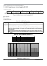
11.3.2.25 Precision Timer Prescaler Select Register (PTPSR)
Read: Anytime
Write: Anytime
All bits reset to zero.
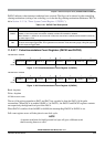
0
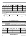
LATQ
Input Control Latch or Queue Mode Enable — The BUFEN control bit should be set in order to enable the IC
and pulse accumulators holding registers. Otherwise LATQ latching modes are disabled.
Write one into ICLAT bit in MCCTL, when LATQ and BUFEN are set will produce latching of input capture and
pulse accumulators registers into their holding registers.
0 Queue mode of Input Capture is enabled. The main timer value is memorized in the IC register by a valid input
pin transition. With a new occurrence of a capture, the value of the IC register will be transferred to its holding
register and the IC register memorizes the new timer value.
1 Latch mode is enabled. Latching function occurs when modulus down-counter reaches zero or a zero is
written into the count register MCCNT (see Section 11.4.1.1.2, “Buffered IC Channels”). With a latching event
the contents of IC registers and 8-bit pulse accumulators are transferred to their holding registers. 8-bit pulse
accumulators are cleared.
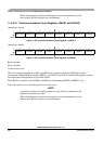
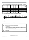
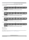
Module Base + 0x002E
76543210
R
PTPS7 PTPS6 PTPS5 PTPS4 PTPS3 PTPS2 PTPS1 PTPS0
W
Reset 00000000
Figure 11-47. Precision Timer Prescaler Select Register (PTPSR)
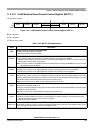
Table 11-31. PTPSR Field Descriptions
Field Description
7:0
PTPS[7:0]
Precision Timer Prescaler Select Bits — These eight bits specify the division rate of the main Timer prescaler.
These are effective only when the PRNT bit of TSCR1 is set to 1. Table 11-32 shows some selection examples
in this case.
The newly selected prescale factorwill not take effectuntil the nextsynchronized edge where all prescale counter
stages equal zero.
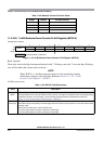
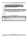
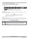
Table 11-32. Precision Timer Prescaler Selection Examples when PRNT = 1
PTPS7 PTPS6 PTPS5 PTPS4 PTPS3 PTPS2 PTPS1 PTPS0
Prescale
Factor
00000000 1
00000001 2
00000010 3
00000011 4
00000100 5
00000101 6
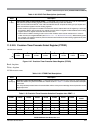
Table 11-30. ICSYS Field Descriptions (continued)
Field Description