


Chapter 4 Port Integration Module (S12XDP512PIMV2)
MC9S12XDP512 Data Sheet, Rev. 2.11
184 Freescale Semiconductor
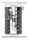
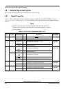
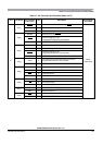
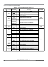
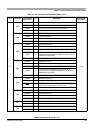
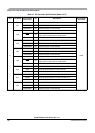
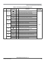
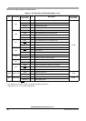
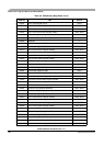
P
PP7
PWM7 I/O Pulse Width Modulator input/output channel 7
GPIO
SCK2 I/O Serial Peripheral Interface 2 serial clock pin
GPIO/KWP7 I/O General-purpose I/O with interrupt
PP6
PWM6 O Pulse Width Modulator output channel 6
SS2 I/O
Serial Peripheral Interface 2 slave select output in master
mode, input for slave mode or master mode.
GPIO/KWP6 I/O General-purpose I/O with interrupt
PP5
PWM5 O Pulse Width Modulator output channel 5
MOSI2 I/O Serial Peripheral Interface 2 master out/slave in pin
GPIO/KWP5 I/O General-purpose I/O with interrupt
PP4
PWM4 O Pulse Width Modulator output channel 4
MISO2 I/O Serial Peripheral Interface 2 master in/slave out pin
GPIO/KWP4 I/O General-purpose I/O with interrupt
PP3
PWM3 O Pulse Width Modulator output channel 3
SS1 I/O
Serial Peripheral Interface 1 slave select output in master
mode, input for slave mode or master mode.
GPIO/KWP3 I/O General-purpose I/O with interrupt
PP2
PWM2 O Pulse Width Modulator output channel 2
SCK1 I/O Serial Peripheral Interface 1 serial clock pin
GPIO/KWP2 I/O General-purpose I/O with interrupt
PP1
PWM1 O Pulse Width Modulator output channel 1
MOSI1 I/O Serial Peripheral Interface 1 master out/slave in pin
GPIO/KWP1 I/O General-purpose I/O with interrupt
PP0
PWM0 O Pulse Width Modulator output channel 0
MISO1 I/O Serial Peripheral Interface 1 master in/slave out pin
GPIO/KWP0 I/O General-purpose I/O with interrupt
Table 4-1. Pin Functions and Priorities (Sheet 5 of 7)
Port Pin Name
Pin Function
and Priority
I/O Description
Pin Function
after Reset