


Chapter 8 Analog-to-Digital Converter (ATD10B8CV3)
MC9S12XDP512 Data Sheet, Rev. 2.11
356 Freescale Semiconductor
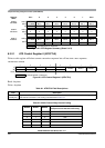
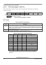
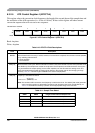
8.3.2.2 ATD Control Register 1 (ATDCTL1)
Writes to this register will abort current conversion sequence but will not start a new sequence.
Read: Anytime
Write: Anytime
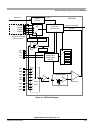
Module Base + 0x0001
76543210
R
ETRIGSEL
0000
ETRIGCH2 ETRIGCH1 ETRIGCH0
W
Reset 00000111
= Unimplemented or Reserved
Figure 8-4. ATD Control Register 1 (ATDCTL1)
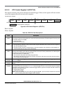
Table 8-3. ATDCTL1 Field Descriptions
Field Description
7
ETRIGSEL
External Trigger Source Select — This bit selects the external trigger source to be either one of the AD
channels or one of the ETRIG3–0 inputs. See the device overview chapter for availability and connectivity of
ETRIG3–0 inputs. If ETRIG3–0 input option is not available, writing a 1 to ETRISEL only sets the bit but has
not effect, that means still one of the AD channels (selected by ETRIGCH2–0) is the source for external trigger.
The coding is summarized in Table 8-4.
2–0
ETRIGCH[2:0]
External Trigger Channel Select — These bits select one of the AD channels or one of the ETRIG3–0 inputs
as source for the external trigger. The coding is summarized in Table 8-4.
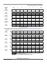
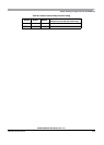
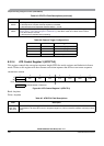
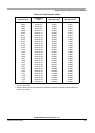
Table 8-4. External Trigger Channel Select Coding
ETRIGSEL ETRIGCH2 ETRIGCH1 ETRIGCH0 External trigger source is
0 0 0 0 AN0
0 0 0 1 AN1
0 0 1 0 AN2
0 0 1 1 AN3
0 1 0 0 AN4
0 1 0 1 AN5
0 1 1 0 AN6
0 1 1 1 AN7
1 0 0 0 ETRIG0
1
1
Only if ETRIG3–0 input option is available (see device overview chapter), else ETRISEL is
ignored, that means external trigger source is still on one of the AD channels selected by
ETRIGCH2–0
1 0 0 1 ETRIG1
1
1 0 1 0 ETRIG2
1
1 0 1 1 ETRIG3
1
1 1 X X Reserved