


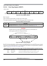
Chapter 23 Memory Mapping Control (S12XMMCV2)
MC9S12XDP512 Data Sheet, Rev. 2.11
898 Freescale Semiconductor
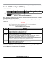
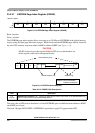
23.3.2.12 RAM Shared Region Upper Boundary Register (RAMSHU)
Read: Anytime
Write: Anytime when RWPE = 0
23.4 Functional Description
The MMC block performs several basic functions of the S12X sub-system operation: MCU operation
modes, priority control, address mapping, select signal generation and access limitations for the system.
Each aspect is described in the following subsections.
23.4.1 MCU Operating Mode
• Normal single-chip mode
There is no external bus in this mode. The MCU program is executed from the internal memory
and no external accesses are allowed.
• Special single-chip mode
This mode is generally used for debugging single-chip operation, boot-strapping or security related
operations. The active background debug mode is in control of the CPU code execution and the
BDM firmware is waiting for serial commands sent through the BKGD pin. There is no external
bus in this mode.
• Emulation single-chip mode
Tool vendors use this mode for emulation systems in which the user’s target application is normal
single-chip mode. Code is executed from external or internal memory depending on the set-up of
the EROMON bit (see Section 1.3.2.5, “MMC Control Register (MMCCTL1)”). The external bus
is active in both cases to allow observation of internal operations (internal visibility).
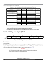
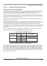
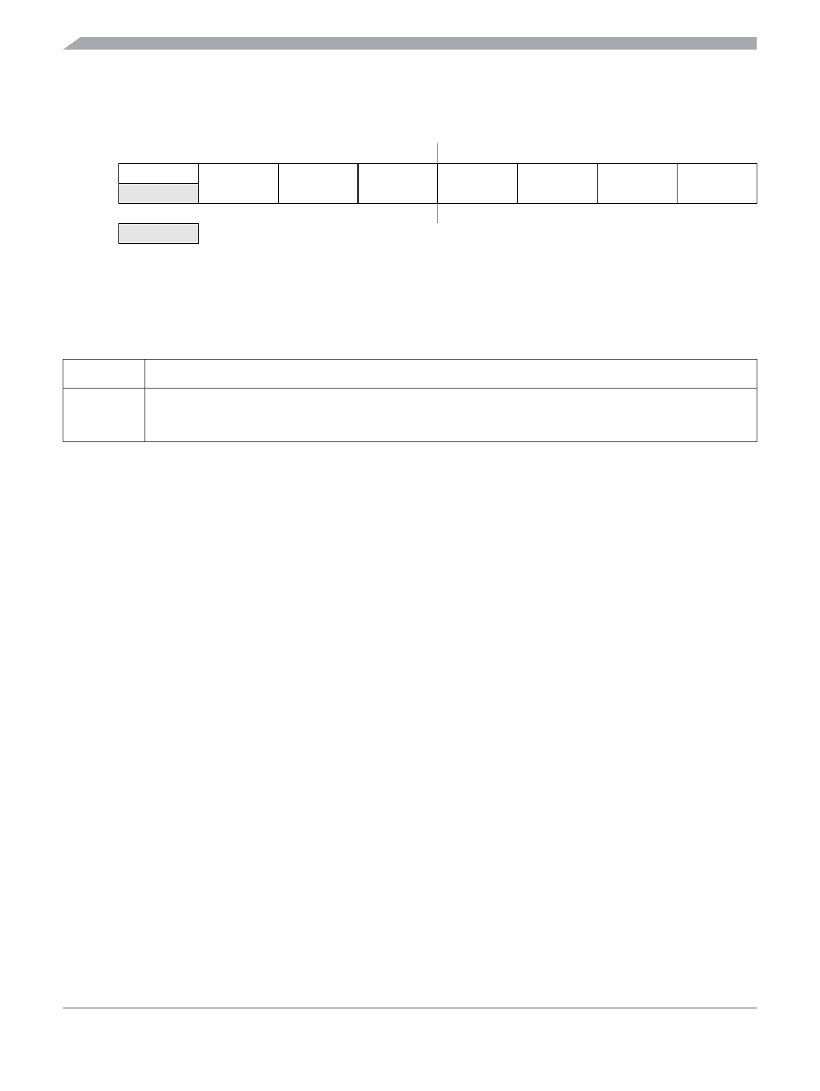
Address: 0x011F
76543210
R1
SHU6 SHU5 SHU4 SHU3 SHU2 SHU1 SHU0
W
Reset 11111111
= Unimplemented or Reserved
Figure 23-20. RAM Shared Region Upper Boundary Register (RAMSHU)
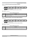
Table 23-17. RAMSHU Field Descriptions
Field Description
6–0
SHU[6:0]
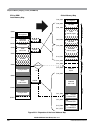
RAM Shared Region Upper Boundary Bits 6–0 — These bits define the upper boundary of the shared
memory in multiples of 256 bytes. The block selected by this register is included in the region. See Figure 1-25
for details.