


Chapter 20 Debug (S12XDBGV2)
MC9S12XDP512 Data Sheet, Rev. 2.11
Freescale Semiconductor 795
20.3 Memory Map and Register Definition
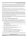
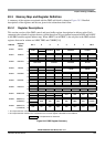
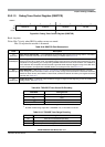
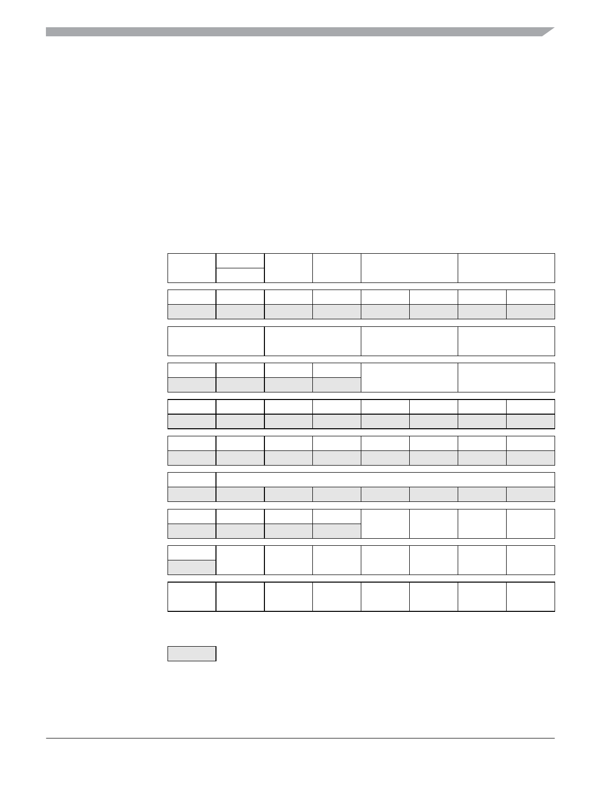
A summary of the registers associated with the DBG sub-block is shown in Figure 20-2. Detailed
descriptions of the registers and bits are given in the subsections that follow.
20.3.1 Register Descriptions
This section consists of the DBG control and trace buffer register descriptions in address order. Each
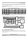
comparator has a bank of registers that are visible through an 8-byte window between 0x0028 and 0x002F
in the DBG module register address map. When ARM is set in DBGC1, the only bits in the DBG module
registers that can be written are ARM, TRIG and COMRV[1:0]
Address
Register
Name
Bit 7 654321Bit 0
0x0020 DBGC1 R
ARM
0
XGSBPE BDM DBGBRK COMRV
W TRIG
0x0021 DBGSR R TBF EXTF 0 0 0 SSF2 SSF1 SSF0
W
0x0022 DBGTCR R
TSOURCE TRANGE TRCMOD TALIGN
W
0x0023 DBGC2 R 0000
CDCM ABCM
W
0x0024 DBGTBH R Bit 15 14 13 12 11 10 9 Bit 8
W
0x0025 DBGTBL R Bit 7 654321Bit 0
W
0x0026 DBGCNT R 0 CNT
W
0x0027 DBGSCRX R 0000
SC3 SC2 SC1 SC0
W
0x0028 DBGXCTL
1
(COMPA/C)
R0
NDB TAG BRK RW RWE SRC COMPE
W
0x0028 DBGXCTL
2
(COMPB/D)
R
SZE SZ TAG BRK RW RWE SRC COMPE
W
1. This represents the contents if the comparator A or C control register is blended into this address
2. This represents the contents if the comparator B or D control register is blended into this address
= Unimplemented or Reserved
Figure 20-2. DBG Register Summary