


Appendix A Electrical Characteristics
MC9S12XDP512 Data Sheet, Rev. 2.11
932 Freescale Semiconductor
A.2 ATD Characteristics
This section describes the characteristics of the analog-to-digital converter.
A.2.1 ATD Operating Characteristics
The Table A-12 and Table A-13 show conditions under which the ATD operates.
The following constraints exist to obtain full-scale, full range results:
V
SSA
≤ V
RL
≤ V
IN
≤ V
RH
≤ V
DDA
.
This constraint exists since the sample buffer amplifier can not drive beyond the power supply levels that
it ties to. If the input level goes outside of this range it will effectively be clipped.
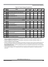
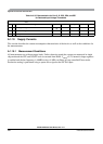
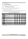
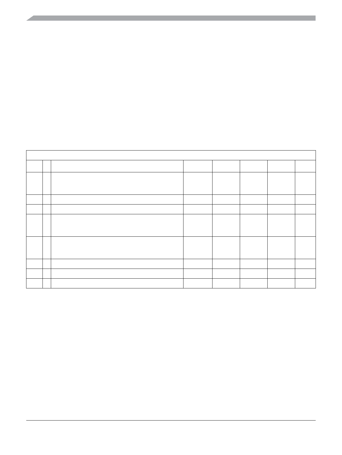
Table A-12. ATD 5-V Operating Characteristics
Conditions are shown in Table A-4 unless otherwise noted, supply voltage 4.5 V < V
DDA
< 5.5 V
Num C Rating Symbol Min Typ Max Unit
1 D Reference potential
Low
High
V
RL
V
RH
V
SSA
V
DDA
/2
—
—
V
DDA
/2
V
DDA
V
V
2 C Differential reference voltage
1
1
Full accuracy is not guaranteed when differential voltage is less than 4.50 V
V
RH
-V
RL
4.50 5.00 5.5 V
3 D ATD clock frequency f
ATDCLK
0.5 2.0 MHz
4 D ATD 10-bit conversion period
Clock cycles
2
Conv, time at 2.0 MHz ATD clock f
ATDCLK
2
The minimum time assumes a final sample period of 2 ATD clocks cycles while the maximum time assumes a final sample
period of 16 ATD clocks.
N
CONV10
T
CONV10
14
7
—
—
28
14
Cycles
µs
5 D ATD 8-Bit conversion period
Clock cycles
2
Conv, time at 2.0 MHz ATD clock f
ATDCLK
N
CONV8
T
CONV8
12
6
—
—
26
13
Cycles
µs
6 D Recovery time (V
DDA
= 5.0 Volts) t
REC
——20µs
7 P Reference supply current 2 ATD blocks on I
REF
— — 0.750 mA
8 P Reference supply current 1 ATD block on I
REF
— — 0.375 mA