


Chapter 17 Voltage Regulator (S12VREG3V3V5)
MC9S12XDP512 Data Sheet, Rev. 2.11
738 Freescale Semiconductor
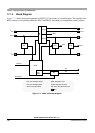
17.2.4 VDDPLL, VSSPLL — Regulator Output2 (PLL) Pins
Signals V
DDPLL
/V
SSPLL
are the secondary outputs of VREG_3V3 that provide the power supply for the
PLL and oscillator. These signals are connected to device pins to allow external decoupling capacitors
(100 nF...220 nF, X7R ceramic).
In Shutdown Mode, an external supply driving V
DDPLL
/V
SSPLL
can replace the voltage regulator.
17.2.5 V
REGEN —
Optional Regulator Enable Pin
This optional signal is used to shutdown VREG_3V3. In that case, V
DD
/V
SS
and V
DDPLL
/V
SSPLL
must be
provided externally. Shutdown mode is entered with VREGEN being low. If VREGEN is high, the
VREG_3V3 is either in Full Performance Mode or in Reduced Power Mode.
For the connectivity of VREGEN, see device specification.
NOTE
Switching from FPM or RPM to shutdown of VREG_3V3 and vice versa
is not supported while MCU is powered.
17.3 Memory Map and Register Definition
This section provides a detailed description of all registers accessible in VREG_3V3.
If enabled in the system, the VREG_3V3 will abort all read and write accesses to reserved registers within
it’s memory slice.
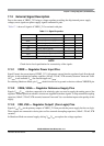
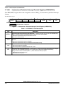
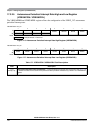
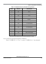
17.3.1 Module Memory Map
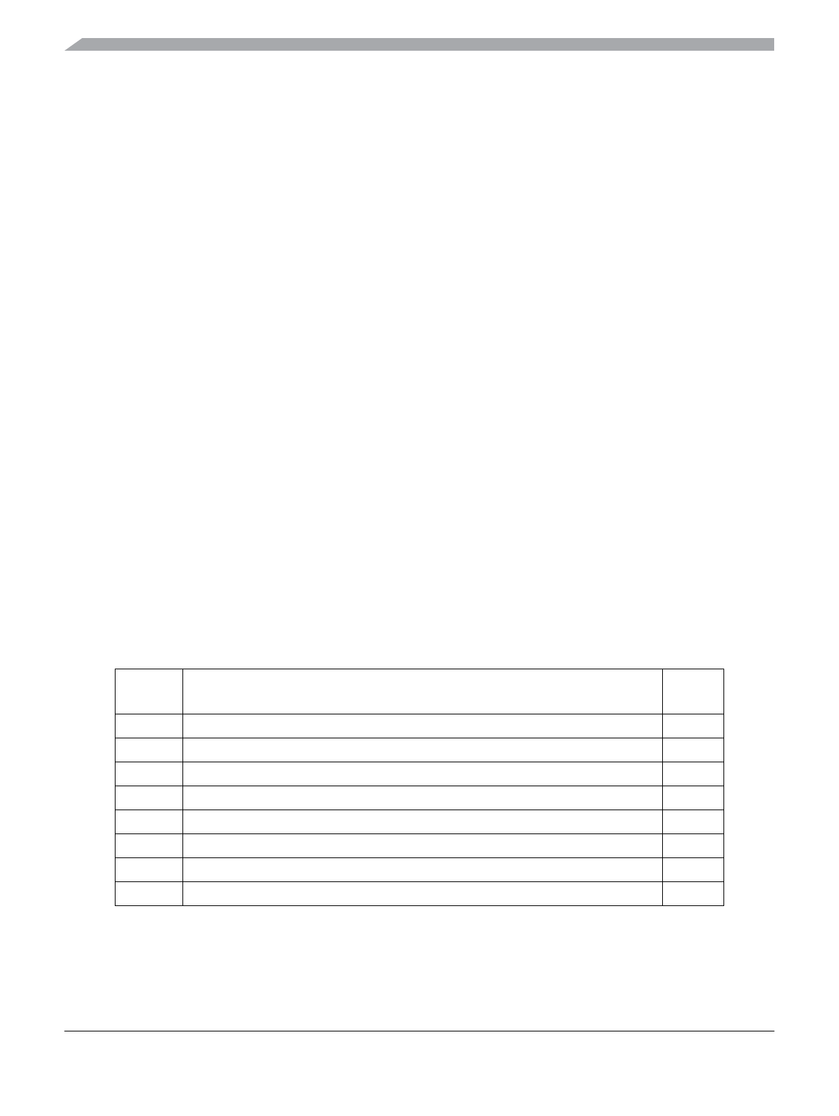
Table 17-2 provides an overview of all used registers.
Table 17-2. Memory Map
Address
Offset
Use Access
0x_00 HT Control Register (VREGHTCL) —
0x_01 Control Register (VREGCTRL) R/W
0x_02 Autonomous Periodical Interrupt Control Register (VREGAPICL) R/W
0x_03 Autonomous Periodical Interrupt Trimming Register (VREGAPITR) R/W
0x_04 Autonomous Periodical Interrupt Period High (VREGAPIRH) R/W
0x_05 Autonomous Periodical Interrupt Period Low (VREGAPIRL) R/W
0x_06 Reserved 06 —
0x_07 Reserved 07 —