


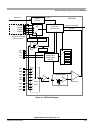


Chapter 8 Analog-to-Digital Converter (ATD10B8CV3)
MC9S12XDP512 Data Sheet, Rev. 2.11
Freescale Semiconductor 357
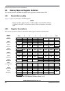
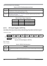
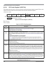
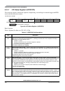
8.3.2.3 ATD Control Register 2 (ATDCTL2)
This register controls power down, interrupt and external trigger. Writes to this register will abort current
conversion sequence but will not start a new sequence.
Read: Anytime
Write: Anytime
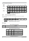
Module Base + 0x0002
76543210
R
ADPU AFFC AWAI ETRIGLE ETRIGP ETRIGE ASCIE
ASCIF
W
Reset 00000000
= Unimplemented or Reserved
Figure 8-5. ATD Control Register 2 (ATDCTL2)
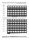
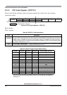
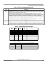
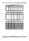
Table 8-5. ATDCTL2 Field Descriptions
Field Description
7
ADPU
ATD Power Up — This bit provides on/off control over the ATD block allowing reduced MCU power
consumption. Because analog electronic is turned off when powered down, the ATD requires a recovery time
period after ADPU bit is enabled.
0 Power down ATD
1 Normal ATD functionality
6
AFFC
ATD Fast Flag Clear All
0 ATD flag clearing operates normally (read the status register ATDSTAT1 before reading the result register to
clear the associate CCF flag).
1 Changes all ATD conversion complete flags to a fast clear sequence. Any access to a result register will
cause the associate CCF flag to clear automatically.
5
AWAI
ATD Power Down in WaitMode — When entering wait mode this bit provides on/off control over the ATD block
allowing reduced MCU power. Because analog electronic is turned off when powered down, the ATD requires
a recovery time period after exit from Wait mode.
0 ATD continues to run in Wait mode
1 Halt conversion and power down ATD during wait mode
After exiting wait mode with an interrupt conversion will resume. But due to the recovery time the result of
this conversion should be ignored.
4
ETRIGLE
External Trigger Level/Edge Control — This bit controls the sensitivity of the external trigger signal. See
Table 8-6 for details.
3
ETRIGP
External Trigger Polarity — This bit controls the polarity of the external trigger signal. See Table 8-6 for
details.
2
ETRIGE
External Trigger Mode Enable — This bit enables the external trigger on one of the AD channels or one of
the ETRIG3–0 inputs as described in Table 8-4. If external trigger source is one of the AD channels, the digital
input buffer of this channel is enabled. The external trigger allows to synchronize sample and ATD conversions
processes with external events.
0 Disable external trigger
1 Enable external trigger
Note: If using one of the AD channel as external trigger (ETRIGSEL = 0) the conversion results for this channel
have no meaning while external trigger mode is enabled.