


Chapter 4 Port Integration Module (S12XDP512PIMV2)
MC9S12XDP512 Data Sheet, Rev. 2.11
260 Freescale Semiconductor
4.4 Functional Description
Each pin except PE0, PE1, and BKGD can act as general purpose I/O. In addition each pin can act as an
output from the external bus interface module or a peripheral module or an input to the external bus
interface module or a peripheral module.
A set of configuration registers is common to all ports with exceptions in the expanded bus interface and
ATD ports (Table 4-67). All registers can be written at any time; however a specific configuration might
not become active.
Example: Selecting a pull-up device
This device does not become active while the port is used as a push-pull output.
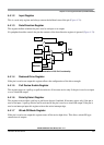
4.4.1 Registers
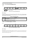
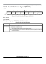
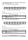
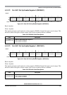
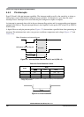
4.4.1.1 Data Register
This register holds the value driven out to the pin if the pin is used as a general purpose I/O.
Writing to this register has only an effect on the pin if the pin is used as general purpose output. When
reading this address, the buffered state of the pin is returned if the associated data direction register bit is
set to “0”.
If the data direction register bits are set to logic level “1”, the contents of the data register is returned. This
is independent of any other configuration (Figure 4-76).
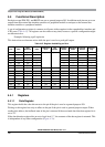
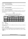
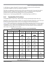
Table 4-67. Register Availability per Port
1
1
Each cell represents one register with individual configuration bits
Port Data
Data
Direction
Input
Reduced
Drive
Pull
Enable
Polarity
Select
Wired-OR
Mode
Interrupt
Enable
Interrupt
Flag
A yes yes — yes yes — — — —
Byesyes— ————
Cyesyes— ————
Dyesyes— ————
Eyesyes— ————
Kyesyes— ————
T yes yes yes yes yes — — — —
S yes yes yes yes yes yes yes — —
M yes yes yes yes yes yes yes — —
P yes yes yes yes yes yes — yes yes
H yes yes yes yes yes yes — yes yes
J yes yes yes yes yes yes — yes yes
AD0 yes yes — yes yes — — — —
AD1 yes yes — yes yes — — — —