


Chapter 4 Port Integration Module (S12XDP512PIMV2)
MC9S12XDP512 Data Sheet, Rev. 2.11
Freescale Semiconductor 211
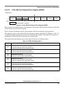
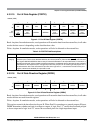
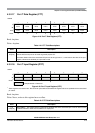
4.3.2.15 Port K Data Register (PORTK)
Read: Anytime. In emulation modes, read operations will return the data from the external bus, in all other
modes the data source is depending on the data direction value.
Write: Anytime. In emulation modes, write operations will also be directed to the external bus.
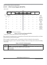
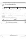
4.3.2.16 Port K Data Direction Register (DDRK)
Read: Anytime. In emulation modes, read operations will return the data from the external bus, in all other
modes the data are read from this register.
Write: Anytime. In emulation modes, write operations will also be directed to the external bus.
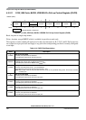
This register controls the data direction for port K. When Port K is operating as a general purpose I/O port,
DDRK determines whether each pin is an input or output. A logic level “1” causes the associated port pin
to be an output and a logic level “0” causes the associated pin to be a high-impedance input.
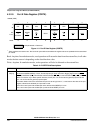
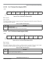
0x0032 (PRR)
76543210
R
PK7 PK6 PK5 PK4 PK3 PK2 PK1 PK0
W
Alt.
Func.
ROMCTL
or
EWAIT
ADDR22
mux
NOACC
ADDR21 ADDR20
ADDR19
mux
IQSTAT3
ADDR18
mux
IQSTAT2
ADDR17
mux
IQSTAT1
ADDR16
mux
IQSTAT0
Reset 00000000
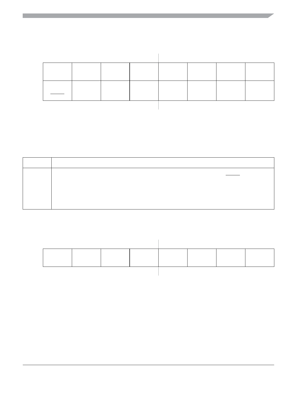
Figure 4-17. Port K Data Register (PORTK)
Table 4-19. PORTK Field Descriptions
Field Description
7–0
PK[7:0]
Port K — Port K pins 7–0 are associated with external bus control signals and internal memory expansion
emulation pins. These include ADDR22-ADDR16, No-Access (NOACC), External Wait (
EWAIT) and instruction
pipe signals IQSTAT3-IQSTAT0. Bits 6-0 carry the external addresses in all expanded modes. In emulation or
special test mode with internal visibility enabled the address is multiplexed with the alternate functions NOACC
and IQSTAT on the respective pins. In single-chip modes the port pins can be used as general-purpose I/O. If
the data direction bits of the associated I/O pins are set to logic level “1”, a read returns the value of the port
register, otherwise the buffered pin input state is read.
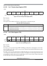
0x0033 (PRR)
76543210
R
DDRK7 DDRK6 DDRK5 DDRK4 DDRK3 DDRK2 DDRK1 DDRK0
W
Reset 00000000
Figure 4-18. Port K Data Direction Register (DDRK)