


Appendix A Electrical Characteristics
MC9S12XDP512 Data Sheet, Rev. 2.11
Freescale Semiconductor 947
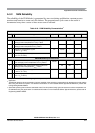
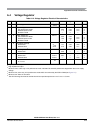
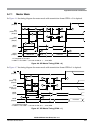
A.5.3 Phase Locked Loop
The oscillator provides the reference clock for the PLL. The PLL´s voltage controlled oscillator (VCO) is
also the system clock source in self clock mode.
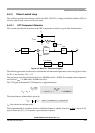
A.5.3.1 XFC Component Selection
This section describes the selection of the XFC components to achieve a good filter characteristics.
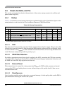
Figure A-3. Basic PLL Functional Diagram
The following procedure can be used to calculate the resistance and capacitance values using typical values
for K
1
, f
1
and i
ch
from Table A-22.
The grey boxes show the calculation for f
VCO
= 80 MHz and f
ref
= 4 MHz. For example, these frequencies
are used for f
OSC
= 4-MHz and a 40-MHz bus clock.
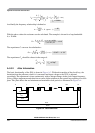
The VCO gain at the desired VCO frequency is approximated by:
The phase detector relationship is given by:
i
ch
is the current in tracking mode.
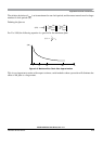
The loop bandwidth f
C
should be chosen to fulfill the Gardner’s stability criteria by at least a factor of 10,
typical values are 50. ζ = 0.9 ensures a good transient response.
f
osc
f
ref
Phase
Detector
VCO
KV
1
synr+1
f
vco
Loop Divider
KF
1
2
D
fcmp
C
s
R
C
p
V
DDPLL
XFC Pin
1
refdv+1
K
V
K
1
e
f
1
f
vco
–()
K
1
1V⋅
----------------------------
⋅=
195MHz V⁄– e
126 80–
195–
--------------------
⋅=
= -154.0MHz/V
K
Φ
i
ch
– K
V
⋅ 3.5µA– 154MHz– V⁄()⋅ 539.1Hz Ω⁄== =