


Chapter 7 Analog-to-Digital Converter (ATD10B16CV4)
MC9S12XDP512 Data Sheet, Rev. 2.11
338 Freescale Semiconductor
7.3.2.12 ATD Input Enable Register 0 (ATDDIEN0)
Read: Anytime
Write: anytime
7.3.2.13 ATD Input Enable Register 1 (ATDDIEN1)
Read: Anytime
Write: Anytime
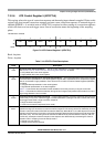
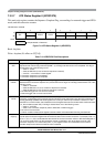
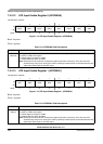
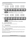
Module Base + 0x000C
76543210
R
IEN15 IEN14 IEN13 IEN12 IEN11 IEN10 IEN9 IEN8
W
Reset 00000000
Figure 7-14. ATD Input Enable Register 0 (ATDDIEN0)
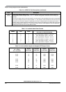
Table 7-23. ATDDIEN0 Field Descriptions
Field Description
7:0
IEN[15:8]
ATD Digital Input Enable on Channel Bits — This bit controls the digital input buffer from the analog input
pin (ANx) to PTADx data register.
0 Disable digital input buffer to PTADx
1 Enable digital input buffer to PTADx.
Note: Setting this bit will enable the corresponding digital input buffer continuously. If this bit is set while
simultaneously using it as an analog port, there is potentially increased power consumption because the
digital input buffer maybe in the linear region.
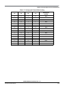
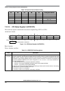
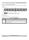
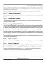
Module Base + 0x000D
76543210
R
IEN7 IEN6 IEN5 IEN4 IEN3 IEN2 IEN1 IEN0
W
Reset 00000000
Figure 7-15. ATD Input Enable Register 1 (ATDDIEN1)
Table 7-24. ATDDIEN1 Field Descriptions
Field Description
7:0
IEN[7:0]
ATD Digital Input Enable on Channel Bits — This bit controls the digital input buffer from the analog input
pin (ANx) to PTADx data register.
0 Disable digital input buffer to PTADx
1 Enable digital input buffer to PTADx.
Note: Setting this bit will enable the corresponding digital input buffer continuously. If this bit is set while
simultaneously using it as an analog port, there is potentially increased power consumption because the
digital input buffer maybe in the linear region.