


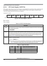
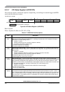
Chapter 8 Analog-to-Digital Converter (ATD10B8CV3)
MC9S12XDP512 Data Sheet, Rev. 2.11
368 Freescale Semiconductor
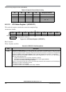
8.3.2.13 ATD Conversion Result Registers (ATDDRx)
The A/D conversion results are stored in 8 read-only result registers. The result data is formatted in the
result registers based on two criteria. First there is left and right justification; this selection is made using
the DJM control bit in ATDCTL5. Second there is signed and unsigned data; this selection is made using
the DSGN control bit in ATDCTL5. Signed data is stored in 2’s complement format and only exists in left
justified format. Signed data selected for right justified format is ignored.
Read: Anytime
Write: Anytime in special mode, unimplemented in normal modes
8.3.2.13.1 Left Justified Result Data
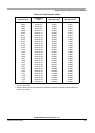
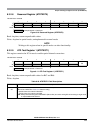
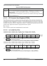
Table 8-22. PORTAD Field Descriptions
Field Description
7–0
PTAD[7:0]
A/D Channel x (ANx) Digital Input (x = 7, 6, 5, 4, 3, 2, 1, 0) — If the digital input buffer on the ANx pin is enabled
(IENx = 1) or channel x is enabled as external trigger (ETRIGE = 1,ETRIGCH[2–0] = x,ETRIGSEL = 0) read
returns the logic level on ANx pin (signal potentials not meeting V
IL
or V
IH
specifications will have an
indeterminate value).
If the digital input buffers are disabled (IENx = 0) and channel x is not enabled as external trigger, read returns
a “1”.
Reset sets all PORTAD0 bits to “1”.
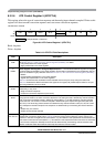
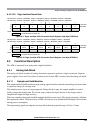
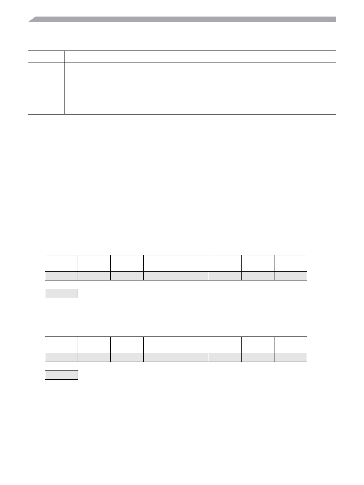
Module Base + 0x0010 = ATDDR0H, 0x0012 = ATDDR1H, 0x0014 = ATDDR2H, 0x0016 = ATDDR3H
Module Base + 0x0018 = ATDDR4H, 0x001A = ATDDR5H, 0x001C = ATDDR6H, 0x001E = ATDDR7H
76543210
R
R
BIT 9 MSB
BIT 7 MSB
BIT 8
BIT 6
BIT 7
BIT 5
BIT 6
BIT 4
BIT 5
BIT 3
BIT 4
BIT 2
BIT 3
BIT 1
BIT 2
BIT 0
10-bit data
8-bit data
W
Reset 0 0 0 0 0 0 0 0
= Unimplemented or Reserved
Figure 8-15. Left Justified, ATD Conversion Result Register, High Byte (ATDDRxH)
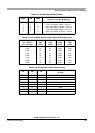
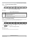
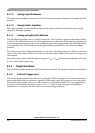
Module Base + 0x0011 = ATDDR0L, 0x0013 = ATDDR1L, 0x0015 = ATDDR2L, 0x0017 = ATDDR3L
Module Base + 0x0019 = ATDDR4L, 0x001B = ATDDR5L, 0x001D = ATDDR6L, 0x001F = ATDDR7L
76543210
R
R
BIT 1
U
BIT 0
U
0
0
0
0
0
0
0
0
0
0
0
0
W
Reset 0 0 0 0 0 0 0 0
= Unimplemented or Reserved
Figure 8-16. Left Justified, ATD Conversion Result Register, Low Byte (ATDDRxL)