


Chapter 11 Enhanced Capture Timer (S12MC9S12XDP51216B8CV2)
MC9S12XDP512 Data Sheet, Rev. 2.11
Freescale Semiconductor 511
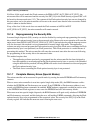
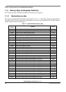
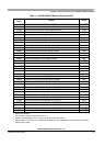
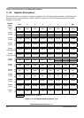
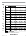
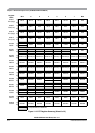
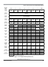
0x001E Timer Input Capture/Output Compare Register 7 High (TC7) R/W
3
0x001F Timer Input Capture/Output Compare Register 7 Low (TC7) R/W
3
0x0020 16-Bit Pulse Accumulator A Control Register (PACTL) R/W
0x0021 Pulse Accumulator A Flag Register (PAFLG) R/W
0x0022 Pulse Accumulator Count Register 3 (PACN3) R/W
0x0023 Pulse Accumulator Count Register 2 (PACN2) R/W
0x0024 Pulse Accumulator Count Register 1 (PACN1) R/W
0x0025 Pulse Accumulator Count Register 0 (PACN0) R/W
0x0026 16-Bit Modulus Down Counter Register (MCCTL) R/W
0x0027 16-Bit Modulus Down Counter Flag Register (MCFLG) R/W
0x0028 Input Control Pulse Accumulator Register (ICPAR) R/W
0x0029 Delay Counter Control Register (DLYCT) R/W
0x002A Input Control Overwrite Register (ICOVW) R/W
0x002B Input Control System Control Register (ICSYS) R/W
4
0x002C Reserved --
0x002D Timer Test Register (TIMTST) R/W
2
0x002E Precision Timer Prescaler Select Register (PTPSR) R/W
0x002F Precision Timer Modulus Counter Prescaler Select Register (PTMCPSR) R/W
0x0030 16-Bit Pulse Accumulator B Control Register (PBCTL) R/W
0x0031 16-Bit Pulse Accumulator B Flag Register (PBFLG) R/W
0x0032 8-Bit Pulse Accumulator Holding Register 3 (PA3H) R/W
5
0x0033 8-Bit Pulse Accumulator Holding Register 2 (PA2H) R/W
5
0x0034 8-Bit Pulse Accumulator Holding Register 1 (PA1H) R/W
5
0x0035 8-Bit Pulse Accumulator Holding Register 0 (PA0H) R/W
5
0x0036 Modulus Down-Counter Count Register High (MCCNT) R/W
0x0037 Modulus Down-Counter Count Register Low (MCCNT) R/W
0x0038 Timer Input Capture Holding Register 0 High (TC0H) R/W
5
0x0039 Timer Input Capture Holding Register 0 Low (TC0H) R/W
5
0x003A Timer Input Capture Holding Register 1 High(TC1H) R/W
5
0x003B Timer Input Capture Holding Register 1 Low (TC1H) R/W
5
0x003C Timer Input Capture Holding Register 2 High (TC2H) R/W
5
0x003D Timer Input Capture Holding Register 2 Low (TC2H) R/W
5
0x003E Timer Input Capture Holding Register 3 High (TC3H) R/W
5
0x003F Timer Input Capture Holding Register 3 Low (TC3H) R/W
5
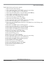
1
Always read 0x0000.
2
Only writable in special modes (test_mode = 1).
3
Writes to these registers have no meaning or effect during input capture.
4
May be written once when not in test00mode but writes are always permitted when test00mode is enabled.
5
Writes have no effect.
Table 11-1. MC9S12XDP512 Memory Map (continued)
Address
Offset
Register Access