


Chapter 20 Debug (S12XDBGV2)
MC9S12XDP512 Data Sheet, Rev. 2.11
Freescale Semiconductor 803
20.3.1.7 Debug State Control Registers
Each of the state sequencer states 1 to 3 features a dedicated control register to determine if transitions
from that state are allowed depending upon comparator matches or tag hits and to define the next state for
the state sequencer following a match. The 3 debug state control registers are located at the same address
in the register address map (0x0027). Each register can be accessed using the COMRV bits in DBGC1 to
blend in the required register (see Table 20-19).
20.3.1.8 Debug State Control Register 1 (DBGSCR1)
Read: Anytime
Write: Anytime when DBG not armed.
This register is visible at 0x0027 only with COMRV[1:0] = 00. The state control register 1 selects the
targeted next state while in State1. The matches refer to the match channels of the comparator match
control logic as depicted in Figure 20-1 and described in Section 20.3.1.11.1, “Debug Comparator Control
Register (DBGXCTL)”. Comparators must be enabled by setting the comparator enable bit in the
associated DBGXCTL control register.
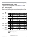
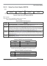
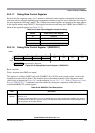
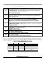
Table 20-19. State Control Register Access Encoding
COMRV Visible State Control Register
00 DBGSCR1
01 DBGSCR2
10 DBGSCR3
11 DBGSCR3
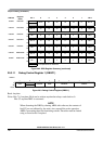
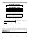
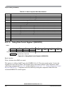
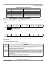
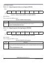
0x0027
76543210
R0000
SC3 SC2 SC1 SC0
W
Reset 00000000
Unimplemented or Reserved
Figure 20-10. Debug State Control Register 1 (DBGSCR1)
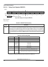
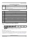
Table 20-20. DBGSCR1 Field Descriptions
Field Description
3–0
SC[3:0}
State Control Bits — These bits select the targeted next state while in State1, based upon the match event.
See Table 20-21.
The trigger priorities described in Table 20-38 dictate that in the case of simultaneous matches, the match on
the lower channel number ([0,1,2,3) has priority. The SC[3:0] encoding ensures that a match leading to final
state has priority over all other matches.