


Appendix A Electrical Characteristics
MC9S12XDP512 Data Sheet, Rev. 2.11
Freescale Semiconductor 921
the injection current may flow out of V
DD35
and could result in external power supply going out of
regulation. Ensure external V
DD35
load will shunt current greater than maximum injection current. This
will be the greatest risk when the MCU is not consuming power; e.g., if no system clock is present, or if
clock rate is very low which would reduce overall power consumption.
A.1.5 Absolute Maximum Ratings
Absolute maximum ratings are stress ratings only. A functional operation under or outside those maxima
is not guaranteed. Stress beyond those limits may affect the reliability or cause permanent damage of the
device.
This device contains circuitry protecting against damage due to high static voltage or electrical fields;
however, it is advised that normal precautions be taken to avoid application of any voltages higher than
maximum-rated voltages to this high-impedance circuit. Reliability of operation is enhanced if unused
inputs are tied to an appropriate logic voltage level (e.g., either V
SS35
or V
DD35
).
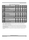
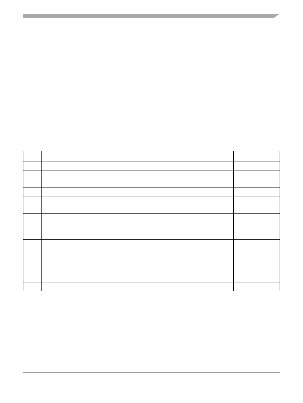
Table A-1. Absolute Maximum Ratings
1
1
Beyond absolute maximum ratings device might be damaged.
Num Rating Symbol Min Max Unit
1 I/O, regulator and analog supply voltage V
DD35
–0.3 6.0 V
2 Digital logic supply voltage
2
2
The device contains an internal voltage regulator to generate the logic and PLL supply out of the I/O supply. The absolute
maximum ratings apply when the device is powered from an external source.
V
DD
–0.3 3.0 V
3 PLL supply voltage
2
V
DDPLL
–0.3 3.0 V
4 Voltage difference V
DDX
to V
DDR
and V
DDA
∆
VDDX
–0.3 0.3 V
5 Voltage difference V
SSX
to V
SSR
and V
SSA
∆
VSSX
–0.3 0.3 V
6 Digital I/O input voltage V
IN
–0.3 6.0 V
7 Analog reference V
RH,
V
RL
–0.3 6.0 V
8 XFC, EXTAL, XTAL inputs V
ILV
–0.3 3.0 V
9 TEST input V
TEST
–0.3 10.0 V
10 Instantaneous maximum current
Single pin limit for all digital I/O pins
3
3
All digital I/O pins are internally clamped to V
SSX
and V
DDX
, V
SSR
and V
DDR
or V
SSA
and V
DDA
.
I
D
–25 +25 mA
11 Instantaneous maximum current
Single pin limit for XFC, EXTAL, XTAL
4
4
Those pins are internally clamped to V
SSPLL
and V
DDPLL
.
I
DL
–25 +25 mA
12 Instantaneous maximum current
Single pin limit for TEST
5
5
This pin is clamped low to V
SSPLL
, but not clamped high. This pin must be tied low in applications.
I
DT
–0.25 0 mA
13 Storage temperature range T
stg
–65 155 °C