


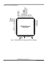
Chapter 1 Device Overview (MC9S12XDP512V2)
MC9S12XDP512 Data Sheet, Rev. 2.11
78 Freescale Semiconductor
NOTE
For devices assembled in 80-pin and 112-pin packages all non-bonded out
pins should be configured as outputs after reset in order to avoid current
drawn from floating inputs. Refer to Table 1-3 for affected pins.
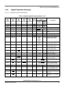
1.2.3 Detailed Signal Descriptions
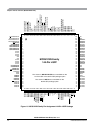
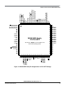
1.2.3.1 EXTAL, XTAL — Oscillator Pins
EXTAL and XTAL are the crystal driver and external clock pins. On reset all the device clocks are derived
from the EXTAL input frequency. XTAL is the crystal output.
1.2.3.2 RESET — External Reset Pin
The RESET pin is an active low bidirectional control signal. It acts as an input to initialize the MCU to a
known start-up state, and an output when an internal MCU function causes a reset.The
RESET pin has an
internal pullup device.
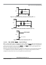
1.2.3.3 TEST — Test Pin
This input only pin is reserved for test. This pin has a pulldown device.
NOTE
The TEST pin must be tied to V
SS
in all applications.
1.2.3.4 V
REGEN
— Voltage Regulator Enable Pin
This input only pin enables or disables the on-chip voltage regulator. The input has a pullup device.
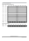
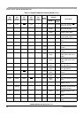
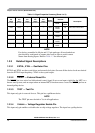
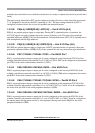
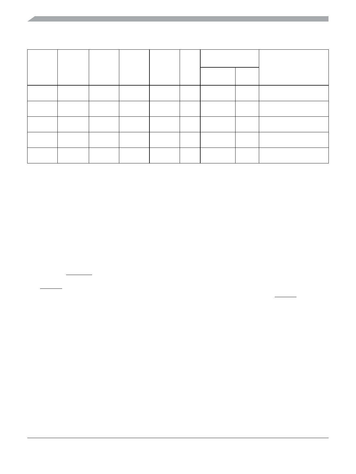
PS3 TXD1 — — — V
DDX
PERS/
PPSS
Up Port S I/O, TXD of SCI1
PS2 RXD1 — — — V
DDX
PERS/
PPSS
Up Port S I/O, RXD of SCI1
PS1 TXD0 — — — V
DDX
PERS/
PPSS
Up Port S I/O, TXD of SCI0
PS0 RXD0 — — — V
DDX
PERS/
PPSS
Up Port S I/O, RXD of SCI0
PT[7:0] IOC[7:0] — — — V
DDX
PERT/
PPST
Disabled Port T I/O, timer channels
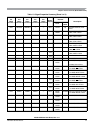
Table 1-3. Signal Properties Summary (Sheet 4 of 4)
Pin
Name
Function 1
Pin
Name
Function 2
Pin
Name
Function 3
Pin
Name
Function 4
Pin
Name
Function 5
Power
Supply
Internal Pull
Resistor
Description
CTRL
Reset
State