


Chapter 11 Enhanced Capture Timer (S12MC9S12XDP51216B8CV2)
MC9S12XDP512 Data Sheet, Rev. 2.11
556 Freescale Semiconductor
If the corresponding NOVWx bit of the ICOVW register is set, the capture register or its holding
register cannot be written by an event unless they are empty (see Section 11.4.1.1, “IC Channels”).
This will prevent the captured value from being overwritten until it is read or latched in the holding
register.
2. IC Queue Mode (LATQ = 0)
The main timer value is memorized in the IC register by a valid input pin transition (see
Figure 11-67 and Figure 11-68).
If the corresponding NOVWx bit of the ICOVW register is cleared, with a new occurrence of a
capture, the value of the IC register will be transferred to its holding register and the IC register
memorizes the new timer value.
If the corresponding NOVWx bit of the ICOVW register is set, the capture register or its holding
register cannot be written by an event unless they are empty (see Section 11.4.1.1, “IC Channels”).
In queue mode, reads of the holding register will latch the corresponding pulse accumulator value
to its holding register.
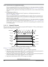
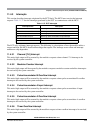
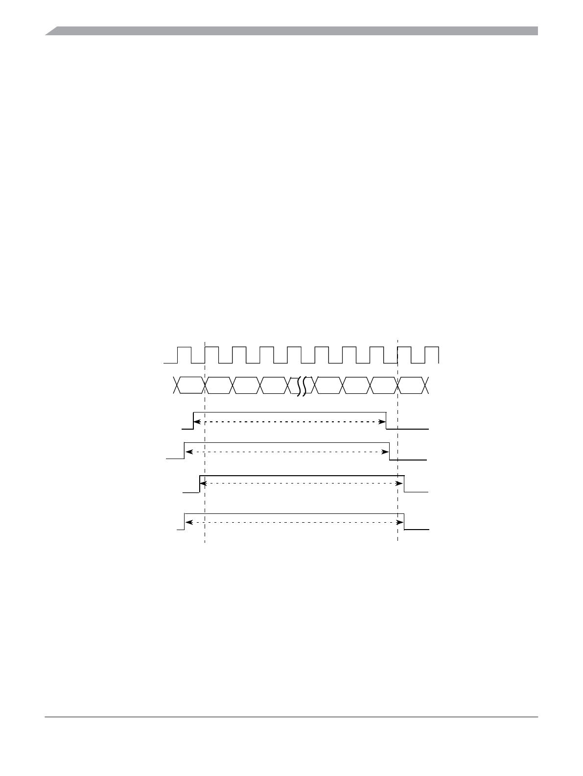
11.4.1.1.3 Delayed IC Channels
There are four delay counters in this module associated with IC channels 0–3. The use of this feature is
explained in the diagram and notes below.
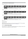
Figure 11-72. Channel Input Validity with Delay Counter Feature
In Figure 11-72 a delay counter value of 256 bus cycles is considered.
1. Input pulses with a duration of (DLY_CNT – 1) cycles or shorter are rejected.
2. Input pulses with a duration between (DLY_CNT – 1) and DLY_CNT cycles may be rejected or
accepted, depending on their relative alignment with the sample points.
3. Input pulses with a duration between (DLY_CNT – 1) and DLY_CNT cycles may be rejected or
accepted, depending on their relative alignment with the sample points.
4. Input pulses with a duration of DLY_CNT or longer are accepted.
1 2 3 253 254 255 256
BUS CLOCK
DLY_CNT
INPUT ON
CH0–3
Rejected
Accepted
INPUT ON
CH0–3
INPUT ON
CH0–3
Accepted
INPUT ON
CH0–3
Rejected
0
255 Cycles
255.5 Cycles
255.5 Cycles
256 Cycles