


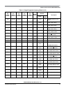

Chapter 1 Device Overview (MC9S12XDP512V2)
MC9S12XDP512 Data Sheet, Rev. 2.11
Freescale Semiconductor 81
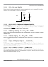
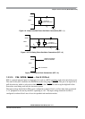
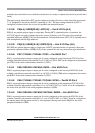
Figure 1-9. Loop Controlled Pierce Oscillator Connections (PE7 = 1)
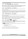
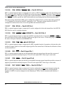
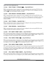
Figure 1-10. Full Swing Pierce Oscillator Connections (PE7 = 0)
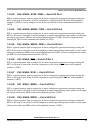
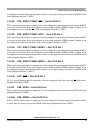
Figure 1-11. External Clock Connections (PE7 = 0)
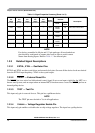
1.2.3.15 PE6 / MODB / TAGHI — Port E I/O Pin 6
PE6 is a general-purpose input or output pin. It is used as a MCU operating mode select pin during reset.
The state of this pin is latched to the MODB bit at the rising edge of
RESET. This pin is an input with a
pull-down device which is only active when
RESET is low. TAGHI is used to tag the high half of the
instruction word being read into the instruction queue.
The input voltage threshold for PE6 can be configured to reduced levels, to allow data from an external
3.3-V peripheral to be read by the MCU operating at 5.0 V. The input voltage threshold for PE6 is
configured to reduced levels out of reset in expanded and emulation modes.
MCU
EXTAL
XTAL
V
SSPLL
Crystal or
Ceramic Resonator
C
2
C
1
MCU
EXTAL
XTAL
R
S
R
B
V
SSPLL
Crystal or
Ceramic Resonator
C
2
C
1
MCU
EXTAL
XTAL
CMOS-Compatible
External Oscillator
Not Connected