


Chapter 16 Serial Peripheral Interface (S12SPIV4)
MC9S12XDP512 Data Sheet, Rev. 2.11
Freescale Semiconductor 727
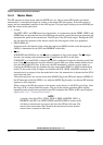
Data reception is double buffered. Data is shifted serially into the SPI shift register during the transfer and
is transferred to the parallel SPI data register after the last bit is shifted in.
After the 16th (last) SCK edge:
• Data that was previously in the master SPI data register should now be in the slave data register and
the data that was in the slave data register should be in the master.
• The SPIF flag in the SPI status register is set, indicating that the transfer is complete.
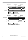
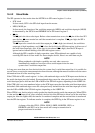
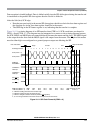
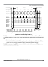
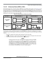
Figure 16-11 is a timing diagram of an SPI transfer where CPHA = 0. SCK waveforms are shown for
CPOL = 0 and CPOL = 1. The diagram may be interpreted as a master or slave timing diagram because
the SCK, MISO, and MOSI pins are connected directly between the master and the slave. The MISO signal
is the output from the slave and the MOSI signal is the output from the master. The
SS pin of the master
must be either high or reconfigured as a general-purpose output not affecting the SPI.
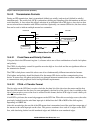
Figure 16-11. SPI Clock Format 0 (CPHA = 0)
t
L
Begin End
SCK (CPOL = 0)
SAMPLE I
CHANGE O
SEL
SS (O)
Transfer
SCK (CPOL = 1)
MSB first (LSBFE = 0):
LSB first (LSBFE = 1):
MSB
LSB
LSB
MSB
Bit 5
Bit 2
Bit 6
Bit 1
Bit 4
Bit 3
Bit 3
Bit 4
Bit 2
Bit 5
Bit 1
Bit 6
CHANGE O
SEL
SS (I)
MOSI pin
MISO pin
Master only
MOSI/MISO
t
T
If next transfer begins here
for t
T
, t
l
, t
L
Minimum 1/2 SCK
t
I
t
L
t
L
= Minimum leading time before the first SCK edge
t
T
= Minimum trailing time after the last SCK edge
t
I
= Minimum idling time between transfers (minimum SS high time)
t
L
, t
T
, and t
I
are guaranteed for the master mode and required for the slave mode.
1 234 56 78910111213141516
SCK Edge Number
End of Idle State Begin of Idle State