


Chapter 8 Analog-to-Digital Converter (ATD10B8CV3)
MC9S12XDP512 Data Sheet, Rev. 2.11
358 Freescale Semiconductor
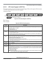
8.3.2.4 ATD Control Register 3 (ATDCTL3)
This register controls the conversion sequence length, FIFO for results registers and behavior in freeze
mode. Writes to this register will abort current conversion sequence but will not start a new sequence.
Read: Anytime
Write: Anytime
1
ASCIE
ATD Sequence Complete Interrupt Enable
0 ATD Sequence Complete interrupt requests are disabled.
1 ATD Interrupt will be requested whenever ASCIF = 1 is set.
0
ASCIF
ATD Sequence Complete Interrupt Flag — If ASCIE = 1 the ASCIF flag equals the SCF flag (see
Section 8.3.2.7, “ATD Status Register 0 (ATDSTAT0)”), else ASCIF reads zero. Writes have no effect.
0 No ATD interrupt occurred
1 ATD sequence complete interrupt pending
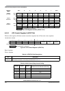
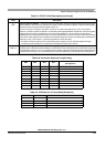
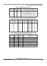
Table 8-6. External Trigger Configurations
ETRIGLE ETRIGP External Trigger Sensitivity
0 0 Falling edge
0 1 Rising edge
1 0 Low level
1 1 High level
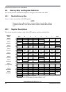
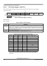
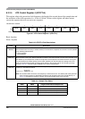
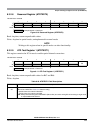
Module Base + 0x0003
76543210
R0
S8C S4C S2C S1C FIFO FRZ1 FRZ0
W
Reset 00000000
= Unimplemented or Reserved
Figure 8-6. ATD Control Register 3 (ATDCTL3)
Table 8-7. ATDCTL3 Field Descriptions
Field Description
6–3
S8C, S4C,
S2C, S1C
ConversionSequence Length — These bits control the number of conversions per sequence. Table 8-8 shows
all combinations. At reset, S4C is set to 1 (sequence length is 4). This is to maintain software continuity to HC12
Family.
Table 8-5. ATDCTL2 Field Descriptions (continued)
Field Description