


Chapter 4 Port Integration Module (S12XDP512PIMV2)
MC9S12XDP512 Data Sheet, Rev. 2.11
182 Freescale Semiconductor
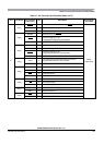
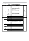
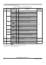
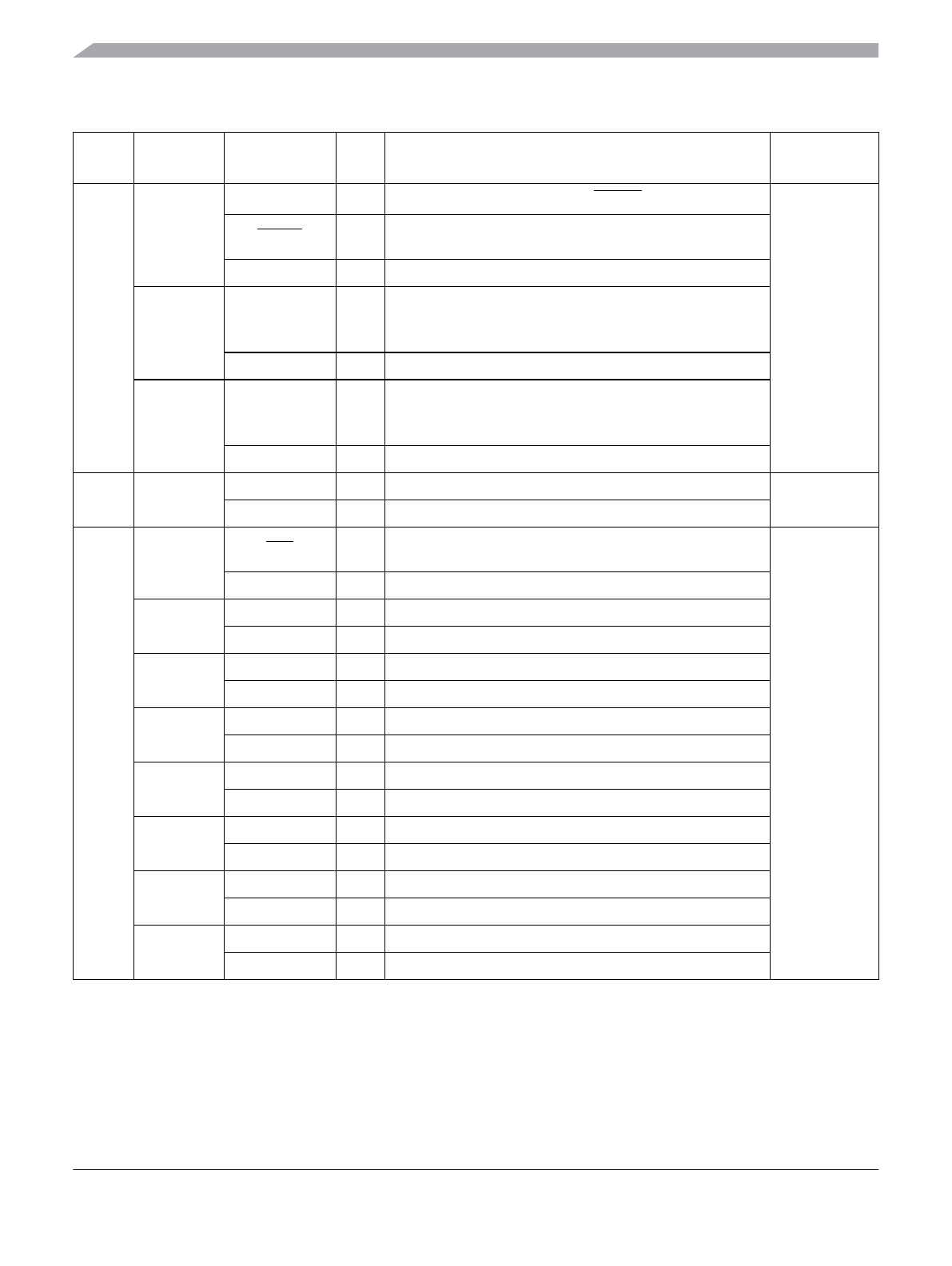
K
PK[7]
ROMCTL
1
I ROMON bit control input during RESET
Mode
dependent
3
EWAIT I
External Wait signal
Configurable for reduced input threshold
GPIO I/O General-purpose I/O
PK[6:4]
ADDR[22:20]
mux
ACC[2:0]
2
O
Extended external bus address output
(multiplexed with access master output)
GPIO I/O General-purpose I/O
PK[3:0]
ADDR[19:16]
mux
IQSTAT[3:0]
2
O
Extended external bus address output
(multiplexed with instruction pipe status bits)
GPIO I/O General-purpose I/O
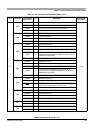
T PT[7:0]
IOC[7:0] I/O Enhanced Capture Timer Channels 7–0 input/output
GPIO
GPIO I/O General-purpose I/O
S
PS7
SS0 I/O
Serial Peripheral Interface 0 slave select output in master
mode, input in slave mode or master mode.
GPIO
GPIO I/O General-purpose I/O
PS6
SCK0 I/O Serial Peripheral Interface 0 serial clock pin
GPIO I/O General-purpose I/O
PS5
MOSI0 I/O Serial Peripheral Interface 0 master out/slave in pin
GPIO I/O General-purpose I/O
PS4
MISO0 I/O Serial Peripheral Interface 0 master in/slave out pin
GPIO I/O General-purpose I/O
PS3
TXD1 O Serial Communication Interface 1 transmit pin
GPIO I/O General-purpose I/O
PS2
RXD1 I Serial Communication Interface 1 receive pin
GPIO I/O General-purpose I/O
PS1
TXD0 O Serial Communication Interface 0 transmit pin
GPIO I/O General-purpose I/O
PS0
RXD0 I Serial Communication Interface 0 receive pin
GPIO I/O General-purpose I/O
Table 4-1. Pin Functions and Priorities (Sheet 3 of 7)
Port Pin Name
Pin Function
and Priority
I/O Description
Pin Function
after Reset