


Chapter 4 Port Integration Module (S12XDP512PIMV2)
MC9S12XDP512 Data Sheet, Rev. 2.11
Freescale Semiconductor 267
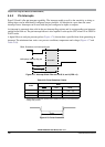
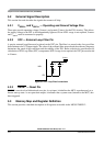
A valid edge on an input is detected if 4 consecutive samples of a passive level are followed by
4 consecutive samples of an active level directly or indirectly.
The filters are continuously clocked by the bus clock in run and wait mode. In stop mode, the clock is
generated by an RC-oscillator in the port integration module. To maximize current saving the RC
oscillator runs only if the following condition is true on any pin individually:
Sample count <= 4 and interrupt enabled (PIE = 1) and interrupt flag not set (PIF = 0).
4.4.4 Expanded Bus Pin Functions
All peripheral ports T, S, M, P, H, J, AD0, and AD1 start up as general purpose inputs after reset.
Depending on the external mode pin condition, the external bus interface related ports A, B, C, D, E, and
K start up as general purpose inputs on reset or are configured for their alternate functions.
Table 4-70 lists the pin functions in relationship with the different operating modes. If two entries per pin
are displayed, a ‘mux’ indicates time-multiplexing between the two functions and an ‘or’ means that a
configuration bit exists which can be altered after reset to select the respective function (displayed in
italics). Refer to S12X_EBI section for details.
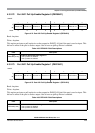
Table 4-70. Expanded Bus Pin Functions versus Operating Modes
Pin
Single-Chip Modes Expanded Modes
Normal
Single-Chip
Special
Single-Chip
Normal
Expanded
Emulation
Single-Chip
Emulation
Expanded
Special
Test
PK7 GPIO GPIO GPIO
or
EWAIT
GPIO GPIO
or
EWAIT
GPIO
PK[6:4] GPIO GPIO ADDR[22:20]
or
GPIO
ADDR[22:20]
mux
ACC[2:0]
ADDR[22:20]
mux
ACC[2:0]
ADDR[22:20]
PK[3:0] GPIO GPIO ADDR[19:16]
or
GPIO
ADDR[19:16]
mux
IQSTAT[3:0]
ADDR[19:16]
mux
IQSTAT[3:0]
ADDR[19:16]
PA[7:0] GPIO GPIO ADDR[15:8]
or
GPIO
ADDR[15:8]
mux
IVD[15:8]
ADDR[15:8]
mux
IVD[15:8]
ADDR[15:8]
PB[7:1] GPIO GPIO ADDR[7:1]
or
GPIO
ADDR[7:1]
mux
IVD[7:1]
ADDR[7:1]
mux
IVD[7:1]
ADDR[7:1]
PB0 GPIO GPIO UDS
or
GPIO
ADDR0
mux
IVD0
ADDR0
mux
IVD0
ADDR0
PC[7:0] GPIO GPIO DATA[15:8]
or
GPIO
DATA[15:8] DATA[15:8] DATA[15:8]
or
GPIO
PD[7:0] GPIO GPIO DATA[7:0] DATA[7:0] DATA[7:0] DATA[7:0]
PE7 GPIO
or
ECLKX2
GPIO
or
ECLKX2
GPIO
or
ECLKX2
ECLKX2 ECLKX2 GPIO
or
ECLKX2